Content last revised on October 5, 2026
Field Diagnostics & Commissioning: Dynamic Gate Impedance Control for Robust CM100TF-12 Topologies
Probe the gate-to-emitter voltage at the module terminals while the opposing switch changes state, and check whether the supposedly off gate rises toward turn-on. This measurement addresses a common commissioning concern: rapid voltage changes can couple into an off-state gate, while voltage developed along a shared emitter return can distort what the driver sees as its reference. Capture the gate waveform together with collector-to-emitter voltage and the driver’s command signal. A gate excursion alone does not establish shoot-through; compare its timing with the current waveform and the commanded switching sequence.
For incoming inspection of a CM100TF-12, identify the terminals from the equipment drawing and the applicable Mitsubishi Electric connection diagram before placing meter leads. With the module disconnected, compare each accessible freewheel path in diode mode against the corresponding path on a known-good assembly. Reverse the leads and record both readings. Check the gate connections separately for unexpected low resistance to the power terminals. Meter readings are screening observations, not substitutes for specified leakage or withstand tests; neither a diode-mode number nor a quiet gate on the bench proves switching performance under load.
💡 Bench Tip: Keep the gate and emitter at the same potential during handling, then record cold diode-mode readings with the same meter and lead orientation used for the reference module.
Design Consideration: An active Miller clamp provides a low-impedance path for unwanted gate charge during the off interval, if the installed driver supports that function. Negative off-state bias is another driver-level approach, but its value cannot be selected from the module’s 600 V and 100 A ratings. Check the driver output limits, gate-emitter limits, supply arrangement and measured gate waveform before changing the bias scheme. Keep the gate-drive return closely associated with its gate path to limit loop pickup, and verify the result at the module terminals rather than relying on a waveform taken only at the driver board.
If a drive trips as switching begins, inspect the gate resistor and driver return for open connections, then look for voltage excursions on the off-state gate during the opposite device’s transition. A resistor change can affect both turn-on behavior and turn-off overvoltage; it is not an isolated cure for a noisy gate. Mitsubishi Electric’s power module technical information provides broader context for relating device switching behavior to driver and circuit conditions, without replacing measurements on the installed assembly.
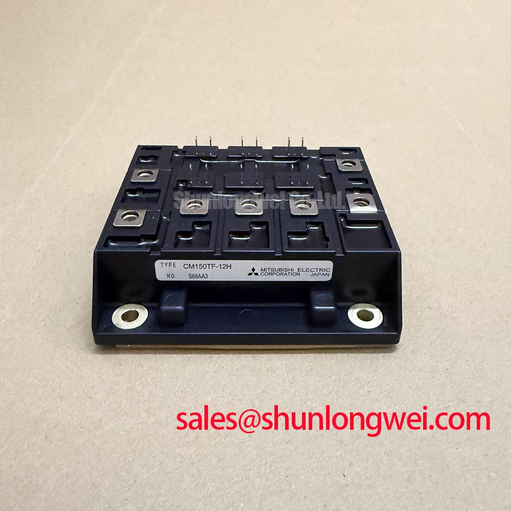
For a maintenance substitution, compare circuit position, terminal arrangement, mounting interface, driver requirements and all relevant ratings before evaluating another part. The CM30TF-12E is a separate model to assess against those requirements, not an assumed drop-in replacement for CM100TF-12. A matching voltage class alone does not establish current capacity or mechanical compatibility.
Field Diagnostics & Commissioning: Optimizing Heatsink Contact Pressure and Surface Fit in CM100TF-12 Topologies
Inspect the heatsink contact pattern when a mounted module runs hotter than expected, and check for untouched areas, trapped debris or displaced thermal interface material. Confirm that the mounting face is clean and that the module seats without rocking. An uneven print of interface material can suggest a contact problem, but temperature also depends on switching duty, cooling airflow and the condition of the surrounding power connections. Record those conditions before attributing a temperature rise to mounting alone.
Design Consideration: Apply thermal interface material as a controlled, continuous film suited to the actual mounting surfaces. Excess material adds a thermal barrier, while gaps interrupt contact. Establish film thickness and the screw-tightening sequence from the applicable mechanical instructions and the heatsink supplier’s requirements; the supplied core specifications do not state a CM100TF-12 film thickness or mounting torque. Tighten mounting points progressively and check that the module remains seated. Do not use screw force to conceal a visibly distorted or damaged mating surface.
Trace the high-side gate supply as a separate check when temperature or trips change with duty cycle. In a bootstrap-fed driver, the capacitor must retain adequate driver supply voltage through the longest interval in which its charging path is unavailable. Engineering Recommendation: Determine its required charge budget from the applicable gate-charge data, driver quiescent draw, leakage and switching pattern, then verify the minimum supply voltage during the actual operating sequence. Check the bootstrap diode’s recovery behavior and the local supply waveform when rapid switching coincides with gate-drive disturbance. Those are driver-circuit decisions; neither bootstrap capacitance nor diode characteristics are specified by the module’s voltage and current ratings.
The same separation matters when inspecting an auxiliary converter or another power switch on the driver supply. An MG100Q1ZS40 may appear in a broader equipment parts assessment, but its role and electrical relationship must be established from that equipment’s schematic rather than inferred from the model names. Where an auxiliary supply uses a buck–boost-derived arrangement, the buck–boost converter operating principles help explain why supply behavior changes with switching conditions. Measure the actual gate-supply rail at the driver before connecting a supply fluctuation to a module fault.
CM100TF-12 Operational Boundaries: Evaluating Thermal Time Constants and Peak Junction Limits
Capture case temperature and collector current during the overload pulse, then compare the pulse history with the cooling interval that follows it. A short pulse can heat the semiconductor faster than the case sensor responds, so a modest case-temperature change does not by itself establish a safe peak junction temperature. Conversely, a case reading taken after shutdown cannot reconstruct the preceding switching losses without the operating waveform.
The 600 V rated voltage and 100 A rated current are Official Specifications for CM100TF-12; they are not a transient thermal impedance curve or permission to exceed a stated operating boundary. For a junction-temperature estimate, Engineering Calculation requires loss over time, an applicable junction-to-case transient thermal model, a measured or bounded case temperature and the operating conditions attached to the source data. A multi-RC model can represent the different time scales of heat flow, but a numerical peak estimate would be unsupported without this model’s verified coefficients and loss characteristics. During troubleshooting, preserve the captured pulse duration, current, voltage and cooling conditions so that a qualified calculation can use the correct event.
Check the gate and collector-emitter waveforms during an overload rather than treating current magnitude as the whole event. A raised on-state collector-emitter voltage may be consistent with overload or loss of adequate gate drive; it is not, by itself, a definitive desaturation diagnosis. If the controller uses desaturation detection and soft turn-off, verify the detection input, blanking behavior and actual turn-off waveform against the installed driver design. Abrupt interruption of fault current can produce a damaging voltage overshoot, while an overly delayed response can increase thermal stress. The permissible short-circuit behavior must come from the applicable device data and circuit verification, not from a generic IGBT timing rule.
Design Consideration: Measure switching peaks under the relevant DC-link condition and compare them with the device’s voltage boundary, allowing for measurement uncertainty and variation in operating conditions. The Ultimate IGBT Knowledge Base is a useful reference for the relationship between switching transients, gate control and thermal loading. It does not supply an installation-specific peak-temperature or safe-operating-area result. Claims about lifetime, altitude effects, cosmic-ray events or failure rates would likewise require applicable device evidence and operating data; none follows from this module’s three supplied core specifications.
In a forklift traction inverter or a bidirectional battery power stage, assess compatibility from the installed circuit and its measured duty cycle. Repeated acceleration, braking and charging transitions can change thermal cycling, but a cycle count or service-life prediction cannot be assigned to CM100TF-12 without characterized losses, temperatures and a supported lifetime model. For a repair record, retain the load profile and temperature observations; these are more actionable than an unsupported life estimate.
CM100TF-12 Circuit Protection & Reliability: Calibrating Overvoltage Trip Prevention via Fast Switching
Record the DC-link voltage and the module’s collector-emitter switching peak during a controlled deceleration event, and note whether the overvoltage trip precedes or follows the braking command. If the bus rises during regeneration, confirm the intended energy path on the equipment schematic. Depending on the installed system, energy may return to a battery or be handled by a braking circuit; the presence of a CM100TF-12 does not establish an internal braking switch or a particular resistor arrangement.
Engineering Recommendation: Size any external braking switch and resistor from the motor and load energy, deceleration profile, DC-link capacitance, permitted bus-voltage range and the braking components’ verified pulse ratings. Check the resistor’s energy and cooling requirements over repeated stops, not just a single event. The required resistance and trip thresholds are system-determined. A resistor selected only to suppress a nuisance trip could overload the switch or resistor under a different stopping duty.
Separate regenerative bus rise from turn-off overshoot in the oscilloscope record. A gradual bus increase points toward an energy-management question, whereas a brief peak aligned with current interruption calls for inspection of the switching loop, gate-drive behavior and nearby connections. Minimize unnecessary power-loop inductance to limit turn-off overshoot, then verify the resulting peak against the measured DC-link voltage during switching tests. Check probe placement and reference routing before acting on a narrow spike that could include measurement-loop pickup.
⚠️ Field Alert: Discharge and verify the DC link before moving probes between the module terminals and the braking circuit.
Finally, check whether an overcurrent event is followed by adequate gate-drive supply recovery before the next commanded transition. A latched trip, a driver undervoltage indication and a bus overvoltage indication call for different follow-up measurements even when each stops the same machine. Preserve the first fault indication and its waveform; repeated restarts can erase the sequence needed to distinguish a protection response from its initiating condition.