Content last revised on September 10, 2026
SCSOA Overcurrent Protection: Implementing Two-Step Gate Voltage Clamping
Field diagnostics on utility-scale 1500V solar central and string inverters frequently trace catastrophic phase-leg failure back to inadequate short-circuit handling. Operating on high-voltage DC links leaves minimal voltage overhead when working with a collector-emitter rating of VCES = 1700V (Official Datasheet Specification). Under typical solar irradiance peaks, high-voltage bus transients combined with stray busbar inductance can elevate terminal voltage during an abrupt fault turn-off. When an inverter bridge encounters a Type-I fault (turning on into an established short) or a Type-II fault (short-circuit occurring while the IGBT is already conducting), the collector current surges beyond the continuous rating of IC = 150A at TC = 112°C (Official Datasheet Specification), driving the silicon into desaturation.
The CM150DU-34KA requires rapid desaturation detection coupled with active gate voltage clamping within the Short-Circuit Safe Operating Area (SCSOA) window. Standard hardware protection circuits measure VCE(sat) across the collector and Kelvin emitter terminals via a high-voltage blocking diode. Given that typical VCE(sat) sits at 3.2V (Typ) at IC = 150A, VGE = 15V (Official Datasheet Specification), the fault detection threshold should be calibrated to trip when forward voltage exceeds 7.0V to 8.5V, allowing for thermal drift under heavy operational loads. Once the desaturation comparator trips, immediately forcing the gate discharge path to snap shut induces an extreme di/dt across the parasitic loop inductance, inevitably producing an overvoltage spike that breaches the 1700V absolute rating.
To safely isolate sub-cycle faults without terminal breakdown, implement a two-step soft turn-off (2-Step STO). When desaturation is validated by the driver IC, the gate potential is stepped down from +15V to an intermediate clamping plateau between 8.0V and 9.5V for roughly 1.5 to 2.5 microseconds. This intermediate step curtails the short-circuit saturation current, reducing di/dt before final zero-volt or negative-bias turn-off completes. When field-validating driver cards after a site shutdown, technicians should consult the standardized surge voltage mapping and gate-clamping verification procedures outlined in the Field Engineer’s Handbook before reconnecting the primary DC link.
Optimizing Heatsink Contact Pressure and Surface Roughness for Minimum R_th(c-s)
Thermal dissipation in high-density 1500V solar topologies is unforgiving. With an internal maximum power dissipation rating of PC = 1100W (Official Datasheet Specification) and a junction-to-case thermal resistance of Rth(j-c)Q = 0.14 °C/W (Official Datasheet Specification), maintaining an unbroken heat flow path from the module baseplate to the extruded aluminum heatsink is critical. Any mechanical deviation that introduces micro-gaps rapidly drives junction temperatures past the maximum operating limits, accelerating silicon degradation.
⚠️ Field Alert: Never apply thermal grease unevenly or overtighten heatsink hardware in an uncontrolled sequence. Baseplate deformation caused by non-uniform torque creates air pockets near the internal ceramic substrate, which can degrade the module's thermal dissipation capability.
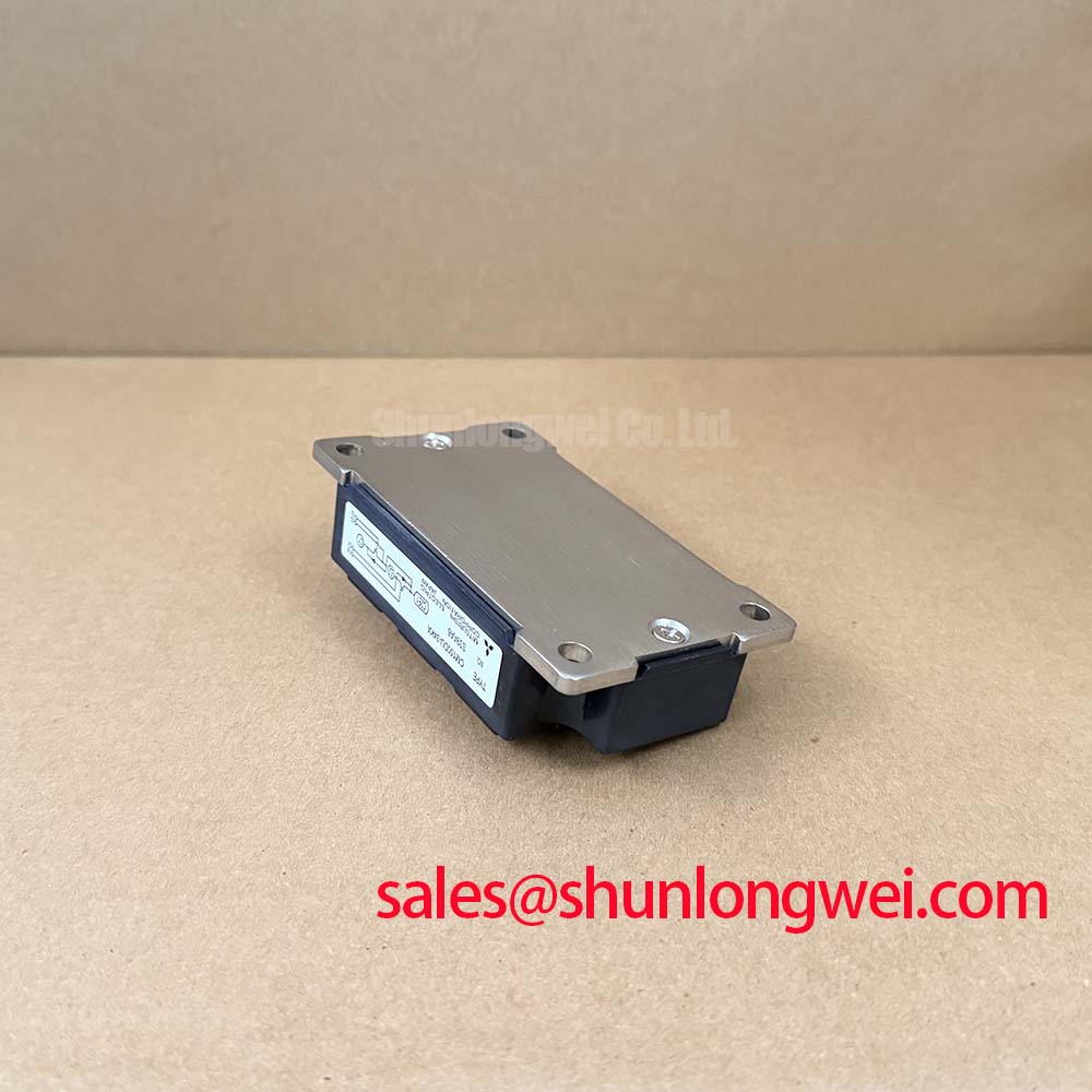
Proper field installation demands rigid mechanical tolerances. The mounting surface must exhibit a flatness deviation within 50 µm over a 100 mm span, with a maximum surface roughness (Rz) of 10 µm. Apply thermal interface material (TIM) using a precision screen printer or a calibrated notched squeegee to achieve an even layer thickness between 60 µm and 80 µm. Once the module is placed on the heatsink, torque application must follow a two-step diagonal sequence: finger-tighten all four mounting screws to approximately 1.0 N·m, then execute the final cross-pattern tightening up to the specified mounting torque of 3.0 to 4.0 N·m. For the main electrical connections, the M6 power terminals require a torque specification of 3.5 to 4.5 N·m (Official Datasheet Specification) to ensure gas-tight interfacial contact without stripping the internal thread inserts.
When engineering inverter auxiliary circuits and protection coordination, compare internal energy handling against high-speed semiconductor fuses. If sub-cycle clearing is required across higher-capacity front-end stages, engineers often benchmark layout parameters against single-switch components such as the CM400HA-12E to isolate fault current energy before it exceeds the thermal limits of the main power bridge.
Optimizing Gate Drive Loop Geometry to Prevent Cross-Conduction Oscillation
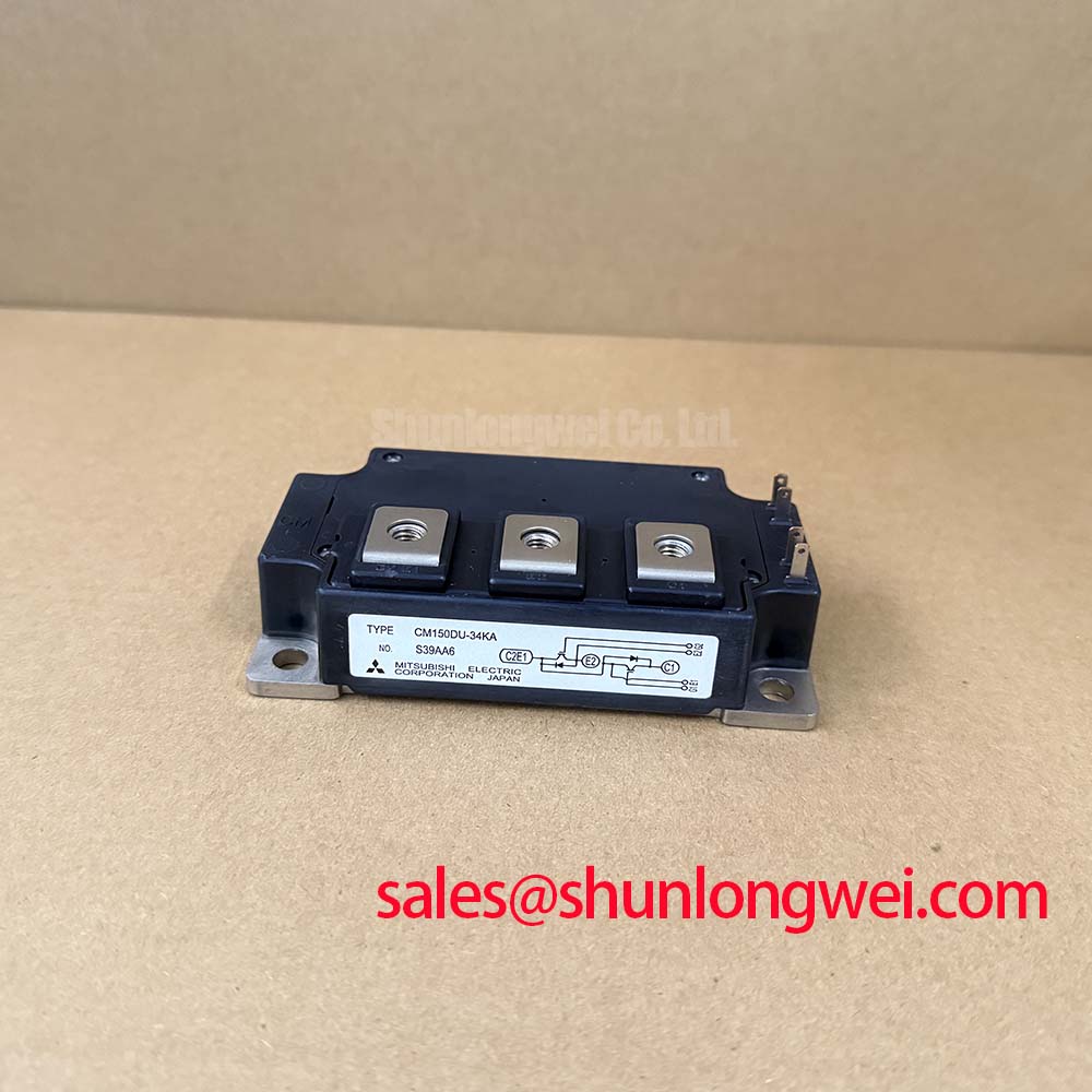
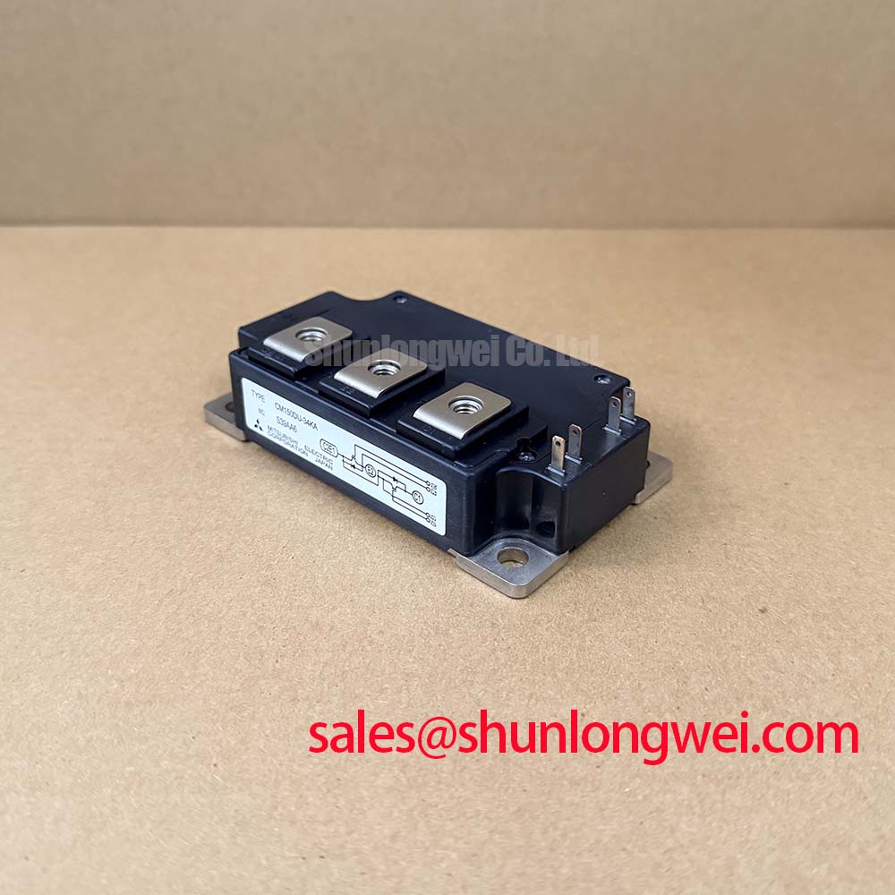
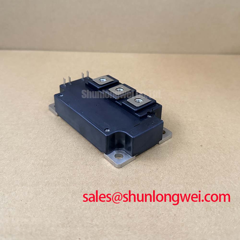
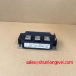
The internal architecture of the CM150DU-34KA incorporates a half-bridge dual structure packaged into a 400g (Official Datasheet Specification) chassis. Driving high-voltage gates safely requires managing substantial capacitive displacement current, as the input capacitance reaches Cies = 21nF (Typ) (Official Datasheet Specification). If board layouts fail to decouple the control circuitry from main power loops, high switched currents couple directly into the gate circuit, inducing parasitic oscillations that lead to simultaneous cross-conduction (shoot-through).
The primary design rule in solar inverter gate drive layouts is the complete isolation of the auxiliary Kelvin emitter terminal from the high-current power emitter path. The auxiliary emitter pin must return exclusively to the gate driver's local reference plane, routed as a tightly coupled differential twisted pair or co-planar stripline with the gate trace. Under rapid load swings, high di/dt flowing through the main busbar generates a mutual inductance voltage drop; if the drive loop shares this path, that voltage directly modulates the gate-to-emitter potential, creating gate ringing that can overcome the gate threshold voltage window of VGE(th) = 5.5V to 8.5V (Official Datasheet Specification).
For systems handling lower DC rail levels where alternative voltage classes are considered, reviewing comparative design layouts using modules such as the CM200DY-24E helps clarify the impact of reduced Miller charge on driver damping circuits. Furthermore, technical documentation on Mitsubishi Electric NX-Series IGBT Modules provides useful reference points regarding baseplate terminal isolation and trace minimization techniques applicable to high-power industrial assemblies.
Common-Mode Transient Immunity (CMTI > 100kV/us) in Harsh Industrial Environments
In 1500V utility-scale solar farms, central and string inverters are exposed to massive common-mode voltage transitions. Fast switching across 1700V DC links generates slew rates exceeding 15 kV/µs. These high dv/dt events induce common-mode currents across the parasitic barrier capacitance of gate driver isolators, which can corrupt logic signals and cause false turn-on pulses on the non-conducting complementary switch.
Maintaining inverter availability requires drive circuitry with Common-Mode Transient Immunity (CMTI) exceeding 100 kV/µs. Gate driver boards paired with the CM150DU-34KA should utilize reinforced galvanic isolation barriers with continuous working voltages rated above 1500V DC and dielectric test certifications exceeding 5.0 kVRMS. Minimizing stray capacitance between the secondary ground plane (referenced to the emitter) and the primary control ground (referenced to the system controller) is essential; keep total coupling capacitance below 2 pF per channel.
Field troubleshooting of phantom phase-leg faults in PV installations should always involve checking for common-mode displacement current leakage. Place a high-frequency current probe around the gate drive signal harness while running diagnostic pulses at reduced bus voltages. If spurious gate-to-emitter noise blips exceed 2.0V during opposite-switch switching events, consider upgrading the driver isolator stage to high-CMTI optocouplers or capacitive isolators with integrated common-mode suppression shields. Using a stiff negative bias (such as -5V to -8V) during the off-state provides critical noise margin, ensuring that induced gate voltage transients remain well below the minimum turn-on threshold under all switching conditions.