Content last revised on September 17, 2026
Benchtop Waveform Tuning: Mitigating Stress via Thermal Paste Degradation Prevention for SKIIP83AHB18T1
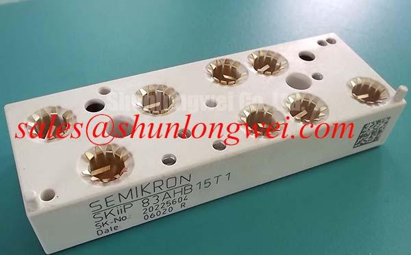
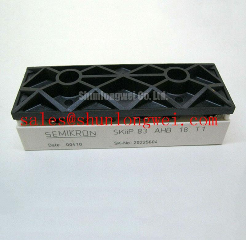
Before connecting gate-drive power, verify the module terminal assignment against the original equipment schematic and inspect the mounting surface for residue, raised burrs, or uneven contact marks. The SKIIP83AHB18T1 is a Semikron intelligent power module with an official 1800 V VCES rating, 100 A nominal collector current, and 200 A maximum collector current. Its three-phase inverter and brake-chopper topology should be confirmed against the existing power-stage connection before replacement work begins.
For a 690 V AC-line inverter, the 1800 V collector-emitter rating provides the documented voltage class, but system engineers should still capture collector-emitter waveforms during switching tests. Stray inductance, DC-link condition, snubber condition, and gate-drive behavior can all affect transient peak voltage. The official typical collector-emitter saturation voltage is 2.1 V at nominal collector current and 25°C, which is relevant when comparing conduction-loss behavior under comparable bench conditions.
Thermal interface material is a Design Consideration rather than an official module thickness specification. A controlled, thin thermal-paste layer can help fill surface irregularities without creating an unnecessarily insulating layer; the appropriate thickness depends on the paste, surface condition, and mounting requirements. Apply paste consistently across the contact region, avoid trapped voids, and use a diagonal screw-tightening sequence so baseplate curvature and heatsink flatness can be accommodated progressively.
💡 Bench Tip: Disconnect and discharge the DC link before handling control or power terminals, then compare cold-state readings with a known-good assembly using the same meter range and probe orientation.
Where a repair investigation includes recurring thermal alarms, inspect the removed interface pattern rather than assuming that the module alone caused the event. Dry, displaced, or unevenly transferred paste may indicate mounting-interface degradation. For broader context on thermal paths and cooling architectures, review The Advanced Thermal Management Revolution.
Assembly Integrity & Layout Architecture: Implementing Dynamic Power Loss Dissipation in SKIIP83AHB18T1
During pulsed overload assessment, distinguish continuous current capability from short-duration current stress. The official ratings identify 100 A as nominal collector current and 200 A as maximum collector current; they do not replace a complete application-level thermal assessment. The specified short-circuit withstand time is 10 μs, allowing a properly designed protection path time to detect and interrupt a fault, subject to the actual gate driver, sensing arrangement, and fault-clearing network.
A multi-RC transient thermal model is an Engineering Calculation method used to estimate junction response during a defined pulse train. Engineers generally combine measured or documented device power loss with the relevant transient thermal impedance curve, case temperature, pulse duration, and repetition pattern. The calculated junction-temperature margin must then be checked against the applicable manufacturer thermal limits from the complete module documentation. This approach is more defensible than treating maximum current as a universal overload setting.
Fuse coordination is also a Design Consideration. A high-speed semiconductor fuse can be evaluated by comparing its clearing behavior and I²t characteristics with the expected fault energy of the complete DC-link circuit. The module’s short-circuit endurance is a protection-response boundary, not a recommendation to permit sustained fault current. Confirm the protection sequence with recorded current and gate signals during controlled validation.
In systems using a separate rectifier or auxiliary conversion stage, engineers may review the electrical role of SKM75GAL063D alongside the inverter architecture. Compatibility depends on the original circuit topology, bus voltage, control strategy, thermal design, and terminal arrangement rather than a part-number relationship alone. Semikron’s MiniSKiiP® power module information provides useful product-family context when reviewing integrated power-module implementations.
Benchtop Waveform Tuning: Mitigating Stress via DC-DC Converter Interleaving and Ripple Current on SKIIP83AHB18T1
For utility-scale centralized battery energy storage PCS evaluations, bidirectional operation can impose alternating power-flow and thermal loading conditions on the inverter bridge. The SKIIP83AHB18T1 combines a three-phase inverter with a brake chopper, so the existing controller must be checked to establish how the chopper path is commanded and monitored during abnormal DC-link conditions. Do not infer gate-drive timing or braking thresholds from the module current rating.
DC-DC interleaving and ripple-current behavior belong to the wider converter design. As a Design Consideration, phase-current ripple, capacitor impedance, switching synchronization, and cable inductance should be measured at the actual DC-link connection points. Excess ripple can contribute to cyclic semiconductor loss and may complicate interpretation of temperature excursions. Oscilloscope measurements should be taken with suitable differential and current probes, with the probe setup verified before comparing one phase with another.
When an alternate legacy Semikron module is being assessed, SKIIP37AC12T4V1 can be reviewed as a separate product record. Engineers should compare voltage class, current ratings, topology, mechanical interface, control-pin arrangement, thermal interface, and original controller requirements before determining whether either unit is suitable for a specific repair evaluation.
Transient suppression components should also be inspected as part of a complete fault review. A metal-oxide varistor can clamp transient energy depending on its installed circuit conditions; the underlying operating principle is described in this reference on varistor transient overvoltage protection. Its presence does not remove the need to verify switching overshoot at the module terminals.
SKIIP83AHB18T1 Circuit Protection & Reliability: Calibrating PCB Gate Loop Layout Symmetry
With the power stage isolated, use a diode-test function only as a comparative static check between corresponding power paths and against the original terminal map. A reading that differs from an equivalent path may indicate a need for further investigation, but meter readings alone cannot establish switching condition, gate-driver health, or dynamic insulation performance. Record probe polarity, meter mode, ambient condition, and the exact terminal pair so later comparisons remain meaningful.
Gate-loop layout is a Design Consideration that becomes especially important when rapid current transitions create shared inductive voltage in the power-emitter return. Keep the gate-drive return path separate from the high-current power return wherever the module terminal arrangement and original design provide an auxiliary reference connection. This reduces common-emitter coupling that can disturb the intended gate-emitter voltage and lead to unequal switching behavior between phases.
Board repairs should preserve symmetry among corresponding gate paths, including the placement and routing of damping, desaturation sensing, isolation barriers, and local decoupling parts. Designers should minimize relevant gate and commutation-loop inductance to suppress turn-off overshoot, then verify peak voltage margins against DC-link voltage with switching tests. The 10 μs short-circuit withstand time remains an official device characteristic, while protection detection delay, gate turn-off response, and fuse action are determined by the finished system.