Content last revised on November 2, 2026
SKM75GB17E4 Operational Boundaries: Evaluating Kelvin Emitter Connection Limits
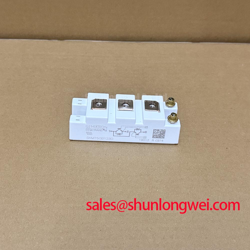
When a replacement module produces irregular gate waveforms or unexplained turn-off ringing, I first separate the auxiliary emitter return from the main high-current emitter path and inspect the complete gate-drive loop. The SKM75GB17E4 from Semikron is specified at VCES = 1700 V and ICnom = 75 A, with a typical VCE(sat) = 1.93 V at 75 A under the datasheet test conditions. The saturation voltage depends on junction temperature and gate-emitter voltage. These ratings identify the electrical class of the device, while the gate-return layout determines how accurately the driver controls switching behavior.
A shared emitter path can develop a voltage difference during rapid collector-current movement. The driver then interprets part of that voltage as a gate signal, which can encourage unwanted oscillation or alter the effective Miller plateau. Keep the auxiliary gate-emitter return routed directly to the driver reference, while the power emitter connection carries the commutation current through its own low-impedance path. Avoid routing the gate loop alongside the collector bus or parallel high-current emitter conductors.
During service testing, compare the gate-emitter waveform at the module terminals with the driver-board reference rather than relying only on a test point several centimeters away. A difference in plateau level, turn-off slope, or ringing frequency may indicate mutual coupling, excessive loop area, or an unsuitable external gate resistor. When evaluating a replacement for a solar inverter power stack, engineers may also review the F4-150R17ME4_B11 as a separate comparison reference, subject to mechanical, electrical, and drive-circuit verification; this does not establish interchangeability.
SKM75GB17E4 Thermal-Electrical Optimization: High-Frequency Commutation Loop Inductance Practical Tuning
High-frequency commutation should be assessed by examining the complete collector-emitter power loop, including the DC-link capacitor connection, module terminals, busbar overlap, and freewheel diode path. The module provides a nominal forward-current rating of IFnom = 75 A and a typical VF = 1.9 V at 75 A under the datasheet test conditions. These figures help establish conduction-loss estimates when the applicable temperature conditions are considered, but switching overshoot remains strongly dependent on circuit inductance, switching speed, temperature, and diode reverse-recovery behavior.
As a Design Consideration, the relationship between turn-off overshoot and stray inductance can be approximated through the engineering expression Vpeak ≈ VDC + Lσ × |di/dt|. The reverse-recovery softness factor of the freewheel diode should be considered alongside its recovered charge because a harder recovery event can increase both voltage overshoot and radiated EMI. Verify the actual waveform with a suitable high-voltage differential probe and place the measurement reference close to the module terminals.
Use a symmetrical planar busbar arrangement where practical, keeping the outgoing and return paths physically close to reduce magnetic loop area. Snubber selection is system dependent: capacitor pulse current, dielectric loss, damping resistance, mounting inductance, and repetitive thermal loading all require bench validation. Gate-drive sourcing and sinking capability should be checked against the selected external RG network. A damping resistor is a Typical Starting Point for tuning, not a universal value for this module.
💡 Pro Tip: Confirm the final busbar and gate-drive arrangement with a controlled switching test before applying the full DC-link voltage.
SKM75GB17E4 Thermal-Electrical Optimization: Baseplate Isolation Breakdown Testing Practical Tuning
Isolation checks should begin with the module disconnected from the driver, busbar, heatsink accessories, and measurement instruments. The official isolation specification is Visol = 4000 V AC at 50 Hz for 1 minute. This withstand-test rating is not a routine service-test instruction. Any terminal-to-baseplate insulation-resistance test voltage, acceptance criterion, and repeat-test procedure should follow manufacturer or equipment-approved maintenance instructions.
Clean the baseplate and surrounding mounting area before testing because conductive dust, moisture residue, and damaged insulating hardware can create surface leakage. Follow the approved test procedure, record the stabilized reading, and discharge the assembly after the test. If the reading changes substantially between repeated tests, inspect the creepage route, mounting washers, terminal contamination, and any trapped debris around the baseplate.
The maximum specified junction temperature is +175 °C; this should not be treated as a recommended continuous operating temperature. That limit does not remove the need to control heatsink flatness, thermal interface condition, clamping uniformity, and enclosure contamination. For broader application context, engineers can consult the Industrial Applications reference when assessing power-module integration in renewable-energy equipment.
SKM75GB17E4 Operational Boundaries: Evaluating Thermal Time Constants and Peak Junction Limits
Peak junction assessment during pulsed overload requires the applied current waveform, conduction interval, switching loss, case temperature, and the manufacturer’s transient thermal impedance data. The relevant calculation uses a multi-RC thermal model to translate time-varying semiconductor loss into junction temperature rise rather than treating the 75 A nominal current as a continuous guarantee under every duty cycle.
For a practical evaluation, capture collector-emitter voltage and current simultaneously, calculate instantaneous power over the pulse, and convolve that power profile with the thermal impulse response derived from the applicable junction-to-case transient thermal impedance. Compare the resulting junction estimate with the datasheet operating limits and the maximum specified Tj of +175 °C, while accounting for heatsink temperature and thermal interface variation. The diode and IGBT should be assessed separately because their conduction and recovery losses and transient thermal responses differ.
When the module is considered for a utility-scale 1500 V central photovoltaic inverter, designers should first verify that the maximum DC-link voltage plus switching overshoot remains within the 1700 V blocking rating with appropriate design margin; the voltage rating alone does not establish suitability. Switching frequency, overload duration, cooling airflow, and protection timing must also be evaluated as a complete system. Reference material from the Semikron-Danfoss Power Modules Catalog and the SEMITRANS® Industry Standard IGBTs range can support device-family and application-level comparison. Gate Miller charge, any active-clamping function, dead-time coordination, and fault detection and shutdown timing should then be verified against the actual driver, protection topology, and device limits.