
Content last revised on October 13, 2026
Transient Dynamics and Electrical Design for CM200DY-12NFA Terminal Joints
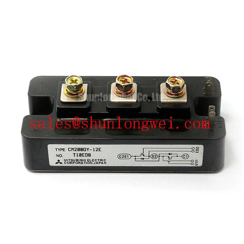
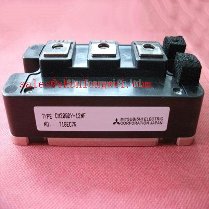
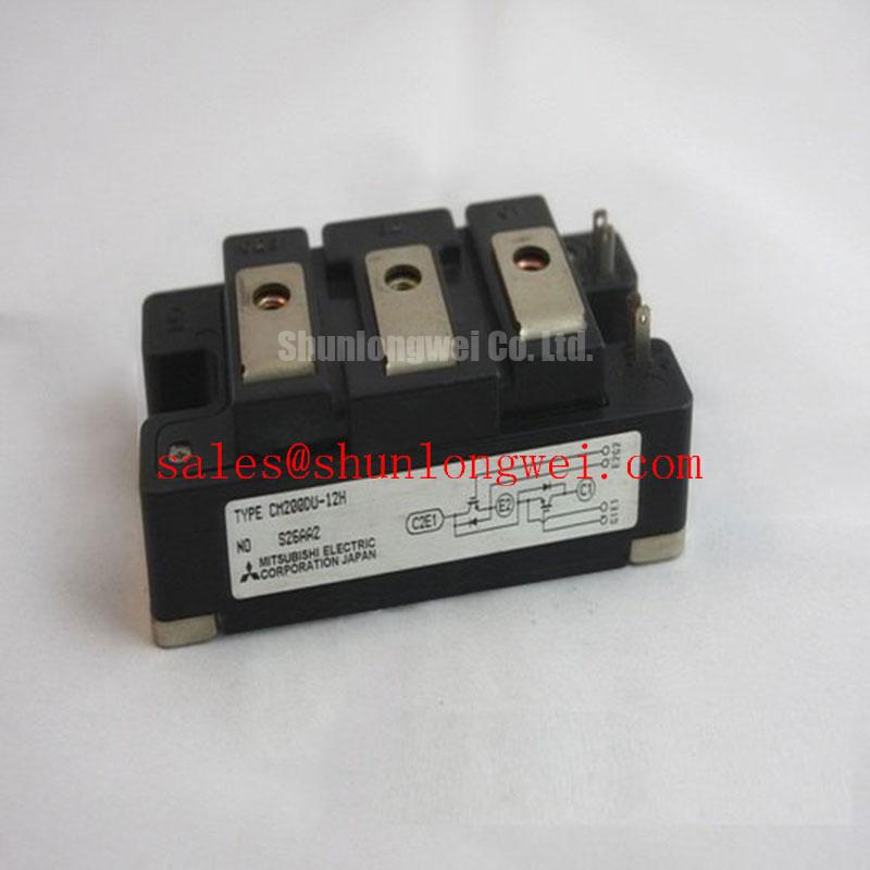
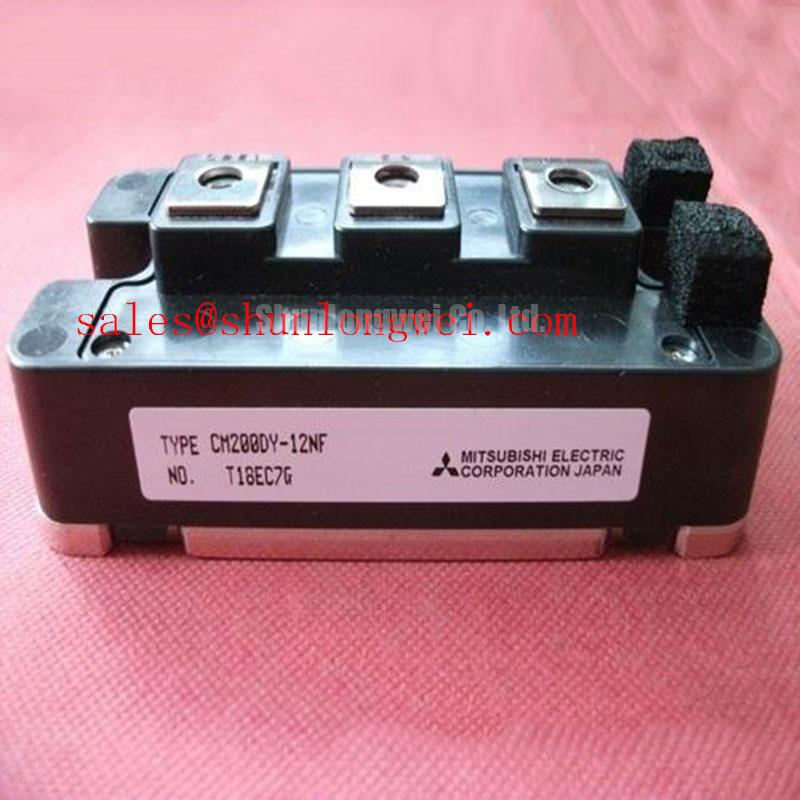
With the variable frequency drive isolated and the DC link safely discharged, start by checking the main terminals for discoloration, loose hardware, and abnormal cold resistance before applying a replacement power module. The CM200DY-12NFA is a Mitsubishi Electric IGBT Module rated at 600.0 V and 200.0 A, with a Module package classification. These are official product specifications and should be matched against the failed unit’s nameplate and the drive manufacturer’s service documentation.
For a heavy duty variable frequency AC motor drive, the practical evaluation is not limited to the semiconductor rating. Terminal condition, commutation loop layout, gate wiring, heatsink contact, output cable behavior, and the protection sequence all influence whether the replacement operates correctly in the existing inverter assembly.
Transient Dynamics and Electrical Design for CM200DY 12NFA Terminal Joints
Bolted contact oxidation deserves immediate attention because a high current path can develop localized heating even when the module itself passes a basic semiconductor check. Clean the mating surfaces according to the equipment service procedure, inspect for pitting or darkened metal, and use a micro ohmmeter with suitable Kelvin connections. As a Design Consideration, the maintenance team may establish a very low joint resistance acceptance criterion, such as less than 10 µΩ, only when the instrument resolution, lead compensation, and test fixture support that measurement.
Record the resistance of each main terminal connection under the same test conditions. A single unusually high reading should be compared with an adjacent connection and with a known good assembly rather than treated as conclusive proof of module failure. Thermographic inspection during a controlled load test can then show whether one bolted joint develops a different thermal profile from the other high current paths.
Keep the power commutation loop compact and physically separated from sensitive gate wiring. The objective is to reduce parasitic inductance that can convert switching current change into turn off overshoot and gate disturbance. Designers should verify the actual peak voltage with a properly referenced oscilloscope setup during switching tests, using the drive’s DC link and protection limits as the system boundary.
Gate loop routing should remain short, symmetrical, and resistant to magnetic coupling from the collector and emitter conductors. The correct gate resistor and damping arrangement are system dependent because driver strength, gate charge, switching frequency, stray inductance, and protection timing all interact. The Mitsubishi Electric IGBT module technical resources provide useful manufacturer context for evaluating module level power device integration.
Operational Boundaries for Output Filters and Motor Cable Reflections
Long motor leads can behave as a transmission line, allowing a fast inverter edge to reflect at the motor terminals. Under unfavorable impedance conditions, the terminal spike can approach twice the applied travelling wave voltage. This is a system level behavior, not a standalone rating of the CM200DY-12NFA, so the cable construction, length, motor input characteristics, switching edge, grounding arrangement, and filter topology must be considered together.
A sinusoidal output filter and a dv/dt reactor do different jobs. A reactor moderates the voltage transition and current ripple seen by the cable, while a sinusoidal filter is intended to produce a waveform closer to a motor friendly sinusoid. The selected network should be verified against the inverter’s switching frequency, motor insulation limits, filter losses, resonance behavior, and protection coordination. Do not substitute one topology for the other based only on the module’s 600 V rating.
| Evaluation point | CM200DY-12NFA | Replacement assessment |
|---|---|---|
| Manufacturer | Mitsubishi Electric | Match the original manufacturer and approved equipment documentation |
| Rated voltage | 600.0 V | Confirm DC link and transient operating conditions in the drive |
| Rated current | 200.0 A | Evaluate load profile, cooling, switching duty, and overload conditions |
| Package | Module | Confirm terminal pattern, mounting interface, and driver compatibility |
For a direct replacement assessment, engineers may also review the neutral listing for CM200DXDX1-24A. This link is provided for comparison only; terminal geometry, electrical ratings, gate drive behavior, and mechanical fit must be checked against the original inverter assembly before any substitution is considered.
Reverse recovery from the freewheeling diode can add current stress and ringing during commutation. Snubber placement, gate resistance, DC link decoupling, and output filtering should be evaluated from measured switching waveforms rather than selected by module current rating alone. An oscilloscope review should cover collector to emitter voltage, gate to emitter voltage, and the current transition at the same operating point. Radiated EMI control depends on the complete enclosure and cable system, so the power module itself should not be represented as independently certified to an EMC standard.
Protection and Reliability Through Baseplate and Heatsink Inspection
Before mounting a replacement, inspect the module baseplate and the heatsink contact surface for burrs, embedded debris, distortion, or uneven wear. A straight edge, calibrated flatness tool, or the equipment manufacturer’s approved inspection method should be used to identify a surface condition that could leave part of the baseplate unsupported.
Thermal interface material should cover the intended contact area as a uniform, thin layer. The appropriate application thickness depends on the selected interface material, application method, surface condition, and compression behavior; follow the material and equipment manufacturer’s instructions. Excess material can increase thermal resistance, while insufficient coverage can create localized hot spots.
Apply the fasteners in a diagonal cross pattern and bring them progressively to the torque specified for the actual screw, washer, heatsink, and equipment assembly. The module package, screw size, thread condition, and heatsink construction determine the acceptable mechanical load. Field Alert: Never use a generic tightening torque or remove the module while the DC link or gate driver remains energized.
After mounting, check that the module sits without rocking and that the power terminals are not being forced into alignment by the busbar. Mechanical stress at the terminal can transfer into the internal structure and may later appear as intermittent switching or thermal instability. Clearance around the busbar and gate wiring should prevent accidental contact during vibration and should preserve the original creepage and insulation arrangement of the drive.
The protection circuit should be checked as a complete chain. Confirm that overcurrent sensing, desaturation or equivalent fault detection, gate shutdown, driver isolation, and fault latching respond in the intended sequence. A protection circuit that reacts too slowly can expose the device to excessive transient stress, while an over sensitive arrangement may cause nuisance trips during normal commutation.
Thermal Electrical Optimization and Current Sharing Adjustment
When IGBT devices operate in parallel, static current sharing is influenced by the positive temperature coefficient of collector emitter saturation voltage. As temperature rises, this characteristic can support a more balanced steady state distribution, but it does not remove the need to match the power path, thermal path, and gate drive layout.
Use equal length and similar geometry for parallel gate connections, keeping the driver reference arrangement consistent for each device. Minimize shared emitter inductance and avoid routing one gate loop beside a high di/dt collector conductor while another loop follows a quieter path. The required gate damping is a Typical Starting Point for bench tuning, not a fixed prescription for every inverter.
During commissioning, compare gate voltage, collector emitter voltage, and current sharing at low stress before progressing toward the normal operating envelope. Look for unequal turn on delay, different turn off ringing, or one branch carrying a visibly different current pulse. These observations may point to driver mismatch, layout asymmetry, connection resistance, or measurement reference error, so the signal path should be checked before changing the gate network.
The associated front end and commutation devices also affect the complete drive topology. Engineers reviewing the rectifier or input stage can place the CM1200HA-34H in the same system level evaluation, without treating it as an automatic companion replacement. For wider power semiconductor design context, the Wide Bandgap Revolution reference discusses switching technology and layout challenges relevant to modern converter development.
For a heavy duty variable frequency AC motor drive, final acceptance should combine cold electrical checks, mechanical inspection, controlled switching observation, thermal imaging, and protection verification. The CM200DY-12NFA remains defined by its official 600.0 V, 200.0 A, Module package specification; the surrounding drive determines how those limits are used in service.