Content last revised on September 12, 2026
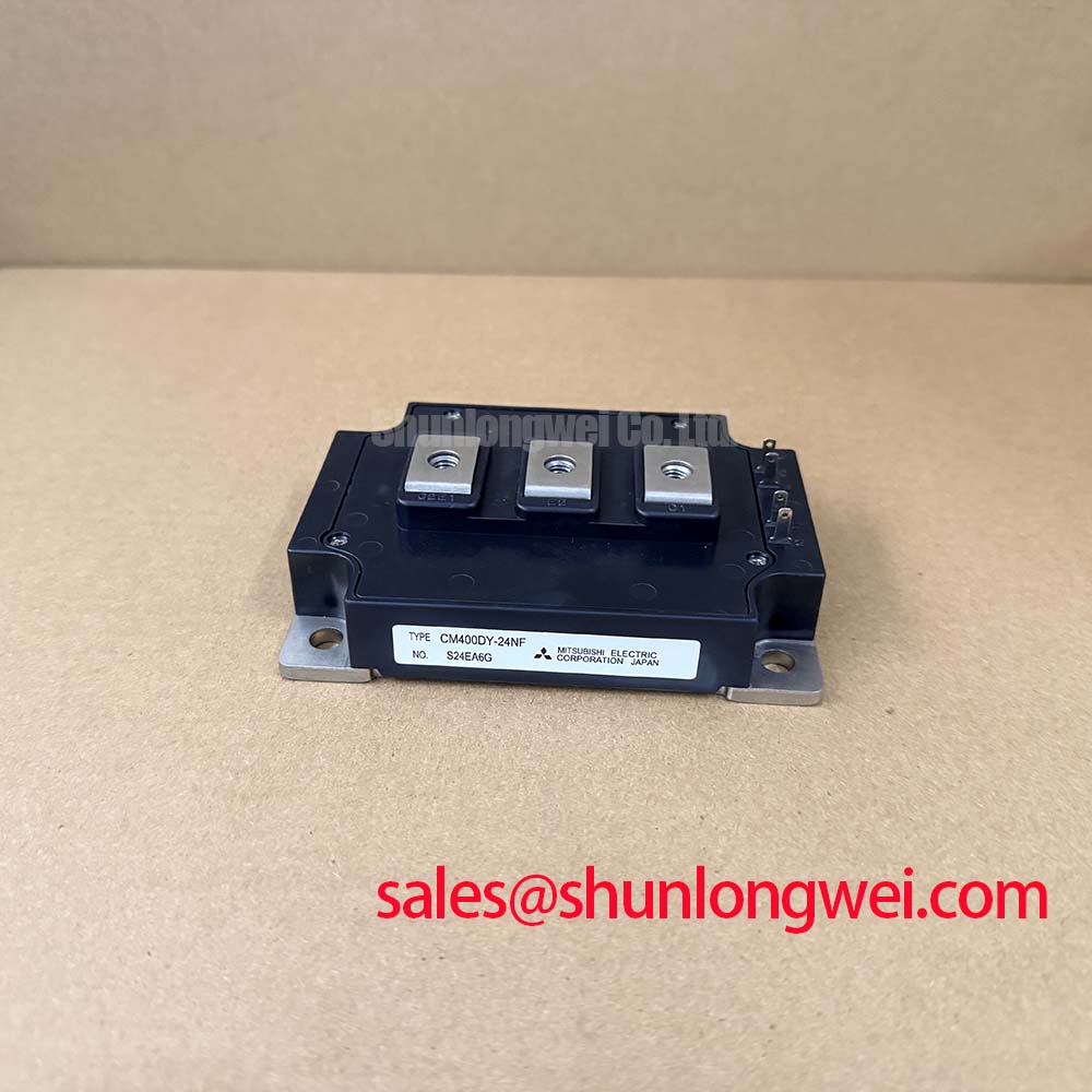
CM400C1Y-24S Mitsubishi Electric 1200V 400A IGBT Module
With the DC link isolated and the module fully discharged, begin incoming inspection by checking the case, terminals, and marked electrical boundaries before connecting any gate-drive or power test equipment. The CM400C1Y-24S is identified here as a Mitsubishi Electric IGBT Module with an official rated voltage of 1200.0 V, an official rated current of 400.0 A, and a Module package. These are product-level specifications supplied for this listing; switching frequency, gate thresholds, short-circuit withstand time, thermal resistance, terminal arrangement, and isolation-test values should be confirmed against the applicable manufacturer documentation before design release.
For a replacement review, compare the original equipment label, mechanical footprint, terminal markings, gate-drive interface, cooling arrangement, and switching behavior. A voltage and current match alone does not establish interchangeability. This is particularly important when evaluating a traction inverter used in high-speed rail or heavy freight locomotive equipment, where bus inductance, gate-driver timing, cooling pressure, and protection coordination are determined by the complete converter assembly.
| Manufacturer | Mitsubishi Electric |
| Part number | CM400C1Y-24S |
| Product category | IGBT Module |
| Rated voltage | 1200.0 V, Official Specification |
| Rated current | 400.0 A, Official Specification |
| Package | Module, Official Specification |
CM400C1Y-24S Circuit Protection & Reliability: Calibrating Active Miller Clamp Implementation
During gate-drive commissioning, first establish the actual terminal identity from the original module documentation and the drive schematic. Do not infer gate, emitter, collector, or auxiliary connections from a visually similar power module. A separate low-impedance gate return can help the driver control the voltage developed by common-source or common-emitter inductance, but the correct connection depends on the module’s documented terminal structure and the driver topology.
High dv/dt at the switching node can transfer current through the opposing device’s Miller capacitance. An active Miller clamp is commonly evaluated as a way to hold the inactive gate at a defined low impedance during this interval. A negative gate bias is also used in some industrial driver architectures, but the values specified in the supplied product information do not confirm a permitted negative gate voltage for this particular part. The system designer should verify the complete gate-emitter operating range from the Mitsubishi Electric device documentation and ensure that the driver never exceeds that boundary during turn-on, turn-off, startup, shutdown, or fault recovery.
Keep the gate-drive loop compact and route the power switching path separately from the sensitive gate-control return. Clearance and creepage should be selected from the working voltage, pollution environment, insulation system, and applicable equipment standard. The layout review should include the driver supply loop, clamp path, gate resistor location, decoupling placement, and the physical relationship between the high-current emitter path and the gate reference. A long shared return can create an apparent gate-voltage disturbance even when the driver output looks clean at its own pins.
For field diagnosis, compare gate-emitter voltage at the module terminals with a known-good switching event while observing the collector-emitter waveform and driver supply. Ringing, delayed turn-off, or an unexpected gate excursion may indicate a layout, probe-ground, driver-saturation, or impedance issue. Verify the measurement setup before changing gate resistance. A Mitsubishi Electric device such as BSM75GD120DLC may be reviewed as a separate replacement candidate when its electrical, mechanical, thermal, and gate-drive requirements have been independently matched; it should not be treated as an automatic substitute.
💡 Bench Tip: Use ESD protection and record the cold-state baseline of every terminal measurement before applying a gate-drive signal, because a test fixture or charged probe can alter the result.
Field Diagnostics & Commissioning: Evaluating Thermal Capacitance vs Heat Sink in CM400C1Y-24S Topologies
Thermal commissioning should start with the complete heat-transfer path rather than with a presumed junction temperature. Confirm the mounting surface, insulation interface if used, thermal interface condition, clamping uniformity, airflow or coolant conditions, and temperature-sensor placement. The supplied product data identifies the package as a module but does not provide a thermal resistance value, transient thermal impedance curve, overload profile, or maximum junction temperature. Those values must come from the applicable technical documentation before a peak-temperature calculation is accepted.
For pulsed overload analysis, engineers commonly represent the junction-to-case response with a multi-time-constant RC network. The useful procedure is to apply the documented power pulse to the relevant transient thermal impedance curve, add the case-temperature boundary, and compare the calculated junction-temperature excursion with the official operating limit. The result is an engineering calculation, not a field-life guarantee. If the thermal curve or pulse conditions are unavailable, use temperature measurements and controlled load testing to establish what the system actually does, then obtain the missing device data before extending the operating envelope.
In parallel-module arrangements, static current sharing should be checked at the actual operating temperature and gate-drive conditions. IGBT forward voltage can exhibit a positive temperature coefficient over a relevant current range, which may support current balancing, but the sharing result still depends on parameter spread, busbar resistance, emitter-path inductance, driver synchronization, and cooling symmetry. Use matched physical routing and symmetrical busbar geometry where practical, then verify individual current paths with appropriately rated sensors or calibrated measurement equipment.
Uneven case temperature does not by itself identify a failed module. Inspect the contact pattern, fastener loading, thermal interface, cooling obstruction, current waveform, and switching losses. A module with a normal cold-state diode measurement can still be affected by dynamic gate-drive or commutation conditions. Conversely, an abnormal bench reading should be repeated with controlled polarity, safe discharge, and a second instrument before a replacement decision is made.
The thermal path should be reviewed alongside the converter’s broader cooling architecture. The article The Advanced Thermal Management Revolution provides useful background on thermal-management concepts, but the CM400C1Y-24S installation must still be validated using its applicable manufacturer data and the equipment-level cooling design.
Benchtop Waveform Tuning: Mitigating Stress via PCB Symmetry Considerations for Dual IGBT on CM400C1Y-24S
On the bench, separate the high-current emitter route from any documented auxiliary or low-inductance gate-return connection. The purpose is to prevent load current from creating a false voltage at the driver reference. If the module does not document an auxiliary emitter terminal, do not add one by assumption. Use the manufacturer’s terminal diagram and the original converter layout to determine which connections are intended for power current and which are intended for control sensing.
Probe placement has a direct effect on the apparent waveform. Measure gate-emitter voltage at the module pins with a suitable differential probe, and measure the collector-emitter waveform with a connection method that minimizes measurement-loop inductance. Confirm probe bandwidth, attenuation, common-mode rating, and reference placement before interpreting overshoot or oscillation. A waveform that appears only after a long probe lead or improvised ground connection may be a measurement artifact rather than a device characteristic.
PCB and busbar symmetry matters when two IGBT positions share a commutation path. Keep the outgoing and return paths physically consistent, avoid routing one gate loop beside a high-amplitude switching node, and place the driver decoupling close to the driver output stage. The target is controlled switching with acceptable voltage overshoot and electromagnetic coupling, while the final gate resistance, dead time, clamp behavior, and switching speed remain system-determined values.
When tuning, change one controlled variable at a time and capture turn-on, turn-off, diode-recovery, startup, and fault waveforms. Check the DC-link voltage at the same operating condition rather than comparing a gate waveform in isolation. If oscillation follows temperature or load current, investigate common-emitter coupling, driver output impedance, supply decoupling, mechanical connections, and commutation-loop layout before assigning the behavior to the CM400C1Y-24S alone. The Mitsubishi Electric Power Semiconductors & High-Power Modules resource is an appropriate manufacturer reference point for broader high-power-module application information.
CM400C1Y-24S Operational Boundaries: Evaluating Desaturation Detection Limits
Desaturation protection is an equipment-level protection function that must be matched to the IGBT module, gate driver, DC-link behavior, and fault-clearing sequence. The supplied CM400C1Y-24S information confirms 1200.0 V rated voltage and 400.0 A rated current, but it does not establish a specific desaturation threshold, blanking interval, short-circuit safe operating area, or guaranteed detection time. Do not present a driver’s commonly used response interval as an official parameter of this module.
In a commissioning test, verify the desaturation sensing path with a controlled low-energy condition before any high-power fault test. Check the sensing diode or network specified by the driver manufacturer, the fault propagation delay, the gate-blocking action, the fault latch, and the reset sequence. A type-I or type-II short-circuit classification should only be used when the applicable module documentation defines that test method and operating condition. Protection timing must be validated against the actual DC-link voltage, stray inductance, gate-drive state, and fault current rise.
A two-stage soft turn-off sequence is often evaluated to reduce the voltage excursion associated with abruptly interrupting a high fault current. Whether that method is suitable depends on the driver implementation and the module’s permitted short-circuit and switching conditions. The system engineer should verify the peak collector-emitter voltage during testing, confirm that the protection circuit reacts before the relevant device limit is exceeded, and ensure that fault energy is not repeatedly accumulated during automatic restart attempts.
If a desaturation event appears during normal switching, inspect the sensing layout, blanking behavior, commutation overshoot, gate-drive supply stability, and current-transfer path. If it fails to appear during a controlled fault test, verify the sensor connection and driver logic with an independent instrument. No single observed symptom establishes a device failure without correlating static measurements, gate waveforms, switching-node behavior, and the equipment protection record. The Mitsubishi Electric Global Semiconductor Device Technologies site should be consulted together with the specific technical documentation required for the final protection design.