Content last revised on September 10, 2026
Incoming Inspection & Parameter Baselines for CM600HB-24A
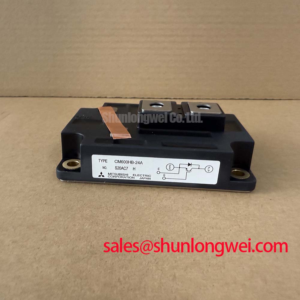
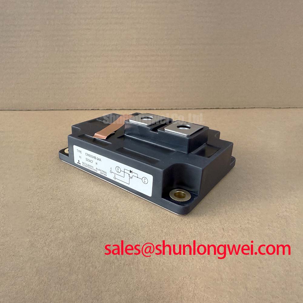
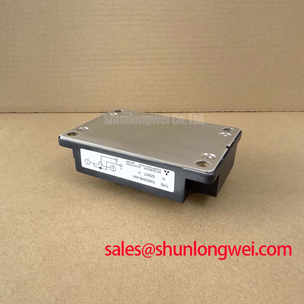
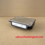
Incoming quality inspection on high-power single-switch modules like the CM600HB-24A begins at the test bench prior to mechanical assembly or high-voltage DC-bus integration. Rated at a continuous collector current of 600A (at TC = 80°C, Official Datasheet Specification) and a collector-emitter blocking voltage of 1200V (Official Datasheet Specification), this medium-power building block serves in multi-megawatt onshore and offshore wind turbine full-scale grid converters. During incoming static screening, bench technicians verify physical package integrity, terminal flatnesses, cold-state junction parameters, and isolation resistance across the copper baseplate to prevent downstream commissioning failures.
Static bench evaluation starts by verifying the integrated anti-parallel free-wheeling diode (FWD) and IGBT collector-emitter channel under non-energized conditions using a calibrated digital multimeter and low-current curve tracer. Between the main collector terminal (Terminal C) and emitter terminal (Terminal E), the integrated diode exhibits a typical cold-state forward conduction drop around 0.35V to 0.45V under standard low-current digital multimeter diode-test range at 25°C ambient. A dual-direction high-impedance check across the gate (Terminal G) and auxiliary emitter (Terminal E) must confirm an open-circuit profile with leakage currents remaining below 0.5 µA at 20V gate-emitter bias (Official Datasheet Specification).
💡 Bench Tip: Before connecting low-impedance gate leads on the incoming inspection bench, maintain an ESD wrist strap grounded to the chassis and keep an anti-static shorting clip across the gate-emitter auxiliary pins until immediately prior to driver board interconnect. The gate oxide layer can be degraded by unmonitored human body model (HBM) electrostatic discharge above 30V even if full dielectric punch-through does not immediately register on a standard curve tracer.
| Parameter Group | Technical Parameter | Specification Value | Classification Standard |
|---|---|---|---|
| Absolute Maximum Ratings | Collector-Emitter Voltage (VCES) | 1200V | Official Datasheet Specification |
| Current Handling | Continuous DC Collector Current (IC) | 600A (at TC = 80°C) | Official Datasheet Specification |
| Saturation Characteristics | Collector-Emitter Saturation Voltage VCE(sat) | 2.1V (Typical at IC = 600A, Tj = 25°C) | Official Datasheet Specification |
| Thermal Metrics | Thermal Resistance Junction-to-Case Rth(j-c) | 0.045 K/W (Maximum IGBT) | Official Datasheet Specification |
| Dynamic Switching | Turn-off Fall Time (tf) | 350ns | Official Datasheet Specification |
Cosmic Ray Robustness: Voltage Derating Curves across 2000m-4000m Altitudes
When wind power converters operate in high-altitude terrain, terrestrial cosmic radiation significantly increases the rate of Single Event Burnout (SEB). High-energy atmospheric neutrons collide with the silicon lattice within the high-field space-charge region of the reverse-biased collector-base junction. This interaction generates localized electron-hole plasma filaments that can trigger unclampable localized thermal runaway. For the CM600HB-24A, maintaining standard sea-level continuous DC-bus operational levels at elevated altitudes without derating risks accelerating unexplained catastrophic failures.
At sea level, an operational DC-bus bias of 750V to 800V represents a standard operational margin for 1200V-class silicon IGBTs. However, empirical atmospheric studies standardized by industry groups like the VDE Association for Electrical, Electronic & Information Technologies show that atmospheric neutron flux density roughly doubles for every 1000 meters of elevation gain above sea level. When multi-megawatt nacelle converter assemblies are deployed at elevations between 2000 meters and 4000 meters, the base Single Event Burnout Failure-In-Time (FIT) rate can rise by more than an order of magnitude if continuous voltage stress remains static.
Mitigating SEB risk requires an active DC-bus headroom reduction strategy rather than relying on standard creepage and clearance extensions alone. For nacelle installations located at 3000 meters, setting the continuous operational DC-link voltage to an upper limit of 650V–680V (Design Consideration for Altitude Derating) lowers the localized electric field below the critical threshold where secondary ionization avalanches become self-sustaining. In multi-level inverter topologies or converter sub-systems operating alongside lower-current bridge legs, such as those employing a CM200DY-24E dual-pack module, engineers balance total series voltage splits across stages to keep per-chip cosmic ray FIT rates within the converter's target mean time between failures (MTBF).
Baseplate Thermal Grease (TIM) Layer Control & Heatsink Mounting Torque Optimization
Thermal heat extraction from the CM600HB-24A depends directly on the mechanical interface between its nickel-plated copper baseplate and the liquid-cooled heatsink cold plate. The maximum junction-to-case thermal resistance Rth(j-c) is specified at 0.045 K/W (Official Datasheet Specification). Maintaining this performance across thermal power cycles in multi-megawatt converters requires tight control over thermal interface material (TIM) thickness, voiding, baseplate convex curvature compensation, and multi-step bolt torquing protocols.
The copper baseplate of a high-power single IGBT module features a intentional slight pre-bow (convex curvature) engineered to flatten out when compressed against the heatsink. If thermal paste is applied too thick, a hydraulic barrier forms, preventing metal-to-metal contact at the baseplate periphery and increasing junction temperatures. Applying the compound using a screen-printing or laser-cut stencil to achieve a target thickness of 50 µm to 100 µm across the module underside ensures complete microscopic void displacement without excessive paste buildup, in accordance with the thermodynamic mechanisms of Thermal Conductance and Thermal Resistance.
⚠️ Field Alert: Fastening module mounting bolts in a single, uncalibrated pass can permanently warp the copper baseplate, crack the internal direct bonded copper (DBC) ceramic substrate, or form air pockets that elevate local thermal resistance by up to 40%. Always follow a symmetrical two-step cross-pattern torque sequence.
When securing the M6 mounting hardware, apply an initial pre-torque of 1.5 N·m to 2.0 N·m across diagonal mounting positions to evenly spread the thermal paste. After a minimum relaxation window of 15 minutes, which allows viscous grease to migrate into micro-grooves, tighten the bolts to the final torque of 3.5 N·m to 4.5 N·m (Design Consideration for M6 baseplate fasteners). High-speed semiconductor fuses installed on the AC and DC terminals must have an I2t clearing rating coordinated lower than the device's maximum short-circuit energy withstand capability, ensuring sub-cycle fault isolation if extreme thermal shock causes thermal gate failure.
Auxiliary Emitter Return Trace Separation for Rapid dv/dt Transients
The switching performance of the CM600HB-24A, with its typical turn-off fall time tf of 350ns (Official Datasheet Specification), generates steep current transitions (di/dt) exceeding 1500 A/µs during high-current interruptions. If the gate driver return path shares conductors with the main power emitter lead, stray inductive coupling introduces parasitic voltages directly into the gate-emitter loop. This dynamic feedback can cause gate ringing, spurious turn-on through the Miller capacitance, or catastrophic bridge-leg shoot-through.
To eliminate this mutual inductance coupling, the module provides a dedicated auxiliary Kelvin emitter terminal isolated physically from the primary high-current emitter lug. The gate driver printed circuit board must route its gate signal and return path as a tightly coupled, differential twisted pair or stripline PCB structure directly to the module's auxiliary gate and emitter terminals. The power stage collector and emitter busbars, which carry up to 600A continuous load current, must remain entirely separate from the low-power driver reference.
In converter topologies utilizing auxiliary half-bridge or boost sub-circuits—where single switches operate alongside medium-current modules like the CM400HA-12E—parasitic loop inductance must be minimized across all parallel trace runs. Inserting an initial gate damping resistor RG of 2.5 Ω to 5.1 Ω (Typical Starting Point for bench tuning) helps suppress ringing caused by parasitic lead inductances and the module's internal input capacitance Cies, stabilizing the switching trajectory under fast dv/dt excursions.
Fault-Clearing Dynamics: Type-I/II Desaturation Detection and Inductive Clamping
Short-circuit conditions in wind turbine grid converters can manifest either as a fault during turn-on into an existing dead short (Type-I Short Circuit) or as an insulation breakdown occurring while the switch is already in the full on-state (Type-II Short Circuit). Under these severe scenarios, the collector current rises beyond rated saturation, pulling the operating point out of the low-loss saturation region into active desaturation. The CM600HB-24A is designed to withstand short-circuit conditions within the short-circuit safe operating area (SCSOA) envelope for a maximum duration of 10 µs.
Desaturation detection circuitry monitors the on-state voltage drop across the collector-emitter terminals. During standard operation at IC = 600A, the typical saturation voltage VCE(sat) remains at 2.1V at 25°C (Official Datasheet Specification). If a short circuit occurs, the voltage across the terminals spikes toward the full DC-link potential. Once the desaturation diode senses a voltage exceeding the typical 6.5V–8.0V reference threshold for longer than an engineered blanking filter time (typically 1.5 µs to 2.5 µs), the driver initiates an emergency fault shutoff.
A conventional rapid gate turn-off under extreme short-circuit fault currents (which can exceed 3000A) will induce an overvoltage spike that exceeds the 1200V VCES limit due to stray loop inductance Lσ. The peak induced voltage corresponds to the product of stray inductance and the rate of current decrease during turn-off, added directly to the nominal DC-bus voltage. To prevent collector-emitter dielectric breakdown, the gate drive must execute a Two-Stage Soft Turn-Off (2STO) or active analog clamping sequence, lowering the gate voltage gradually over 2 µs to 4 µs to moderate the di/dt trajectory.
Field maintenance technicians and converter design engineers diagnosing repeated overcurrent trips or desaturation anomalies can consult practical troubleshooting workflows and structural root-cause isolation techniques outlined in the Field Engineer’s Handbook for power semiconductor validation.