

Content last revised on September 26, 2026
FP100R07N3E4 DC Bus Layout and Turn-Off Overshoot
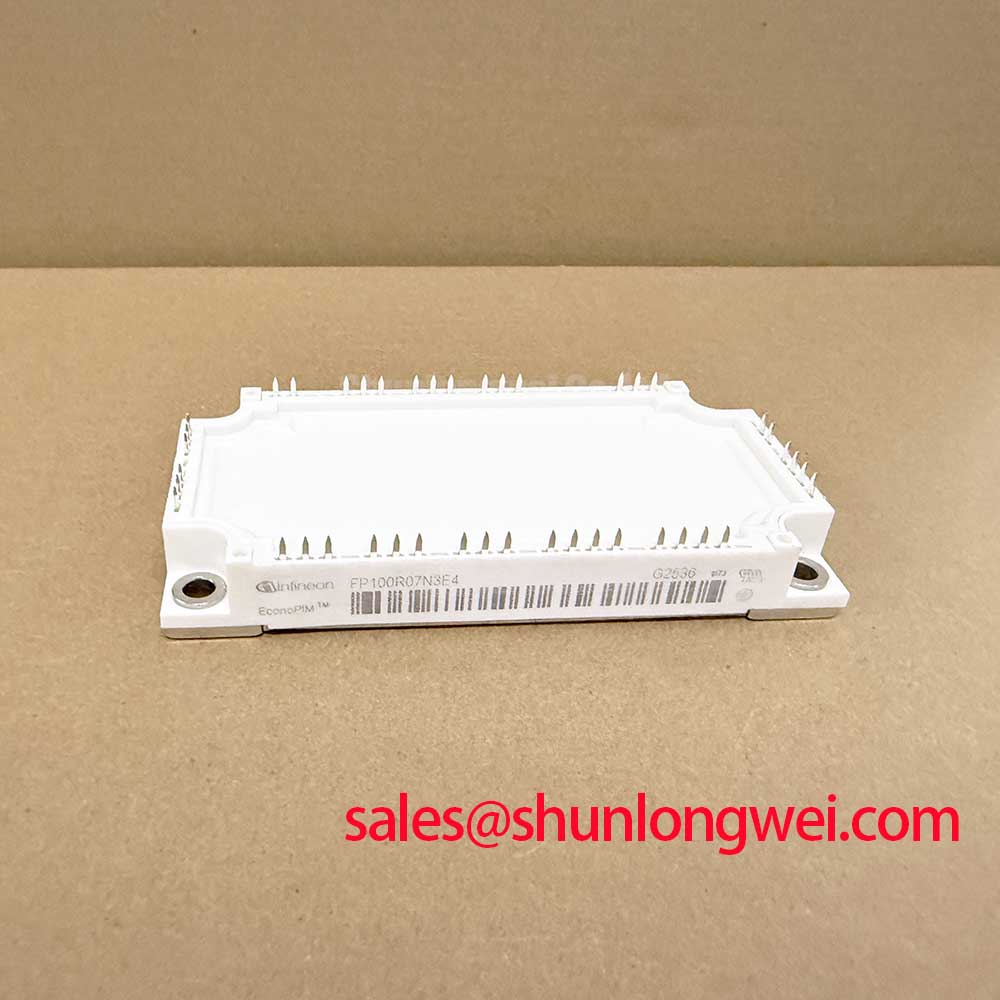
With the DC bus discharged and verified safe, compare the cold terminal readings of the failed assembly with the equipment schematic before fitting an FP100R07N3E4. Identify the inverter, rectifier, brake chopper and temperature sensor connections first; a meter reading is useful for screening an obvious short, but it cannot establish switching health or prove that a different module will fit.
The FP100R07N3E4 is an Infineon IGBT module with four documented function groups. Its inverter IGBT has a 650 V collector-emitter voltage rating, its rectifier diode has an 800 V repetitive peak reverse voltage rating, its brake chopper IGBT has a 650 V collector-emitter voltage rating, and its temperature sensor has an R25 value of 5 kΩ. These are official specification values for the respective functions, not interchangeable ratings for every terminal.
| Function | Official specification | Check in the equipment |
|---|---|---|
| Inverter IGBT | VCES: 650 V | Confirm DC-link and switching-peak compatibility. |
| Rectifier diode | VRRM: 800 V | Confirm the diode’s location and reverse-voltage duty in the schematic. |
| Brake chopper IGBT | VCES: 650 V | Check the brake circuit and its protection path. |
| Temperature sensor | R25: 5 kΩ | Check that the controller expects this sensor characteristic. |
A laminated busbar can shorten the commutation path, but its presence alone does not establish an acceptable switching peak. As a Design Consideration, minimize the loop between the DC-link capacitors and the switching terminals to limit inductive overshoot during turn-off. The voltage at the device rises with DC-link voltage and the product of loop inductance and current slew rate; the equipment designer must measure that peak under its operating conditions and compare it with the relevant device rating. Busbar geometry, insulation spacing and any snubber selection must be checked against the complete assembly rather than assigned a universal target.
On a stopped machine, inspect busbar seating, fastener condition, insulating surfaces and capacitor connections before attributing a trip to the module. A loose or changed current path may alter the waveform, while an inverter fault can also originate in the gate drive, load or protection circuit. When power-up testing is authorized, capture the DC-link voltage and switching transient with an appropriately rated measurement setup. Record where the probe reference is connected: a long measurement loop can make a transient appear worse than it is.
For equipment that combines rectification and inverter functions, follow the actual power-path drawing instead of assuming that another module performs the same role. The FS100R12N2T4 can be examined as a separate module in a wider power-stage assessment, but its ratings, topology and terminal arrangement require their own documentation before any integration decision.
FP100R07N3E4 Output Transients and Gate Timing
If a drive trips after a motor cable or output assembly has been changed, inspect the load connection and measure the waveform at the equipment terminals. Cable reflections and impedance mismatch are system effects; they cannot be assigned a fixed voltage multiplier for this module without the cable, load and switching conditions. As a Design Consideration, an output filter or choke may be evaluated where measured terminal stress warrants it. Its selection belongs to the equipment design and must account for switching behavior, load current and thermal effects.
Separate output-terminal measurements from measurements at the IGBT terminals. A reflected pulse on a long cable and a DC-bus commutation overshoot call for different checks, even if both appear during the same switching event. Inspect the original output network, cable routing and connections before changing components. For a possible industrial inverter welder or medium-frequency induction-heating supply, first establish the actual load topology; neither application name establishes compatibility with FP100R07N3E4.
Complementary gate commands also need an interval that prevents simultaneous conduction. That interval cannot be prescribed from the ratings listed here. Check the controller command, driver output and device-terminal waveforms in sequence, then assess dead time across the operating conditions specified by the equipment designer. If the command waveforms are correctly separated but current rises unexpectedly, inspect gate return routing, driver supply behavior and the power path before assigning a single cause.
For a replacement assessment, compare more than the model name and headline voltage. Confirm the original circuit’s terminal mapping, rectifier and brake functions, sensor input, mechanical interface and applicable switching limits. The BSM100GAL100D is a separate comparison candidate for a documented engineering review, not an assumed drop-in substitute; its specifications and physical connections must be checked independently.
High dv/dt Gate Coupling and Cross-Conduction Checks
A rapid collector-voltage change can couple into an IGBT gate circuit. That physical mechanism is relevant when an off-state device appears to turn on during its complementary device’s switching transition, but a current spike alone does not prove Miller-induced cross-conduction. Capture the gate-to-emitter voltage at the device connections alongside the switching waveform, using measurement methods appropriate to the live bus. Compare the result with the driver command and the equipment’s known-good channel where available.
As a Design Consideration, keep the gate-drive and return paths controlled so that power-current transients do not create an unintended gate signal. Driver features such as an active Miller clamp can be evaluated against the original gate circuit. Any off-state gate bias must be established from the module and driver documentation and validated by the system engineer; the specifications supplied here do not establish a negative-bias value or a gate-resistor setting.
Check the gate harness, connector seating and driver reference before replacing a power module in response to an intermittent overcurrent trip. Review whether the observed gate disturbance coincides with a command transition, a bus transient or a protection event. Infineon’s IGBT and co-pack diode information provides background on IGBT switching behavior, but device-family guidance is not a substitute for the FP100R07N3E4 pinout and switching specifications. Infineon’s low-voltage MOSFET information describes a different device category and should not be used to infer this IGBT module’s gate limits.
FP100R07N3E4 Assembly and Overcurrent Protection Verification
Before mounting the module, inspect the contact surfaces, locating features, terminals and cooling interface. Match the equipment’s fasteners and tightening procedure to its service documentation, and check that the busbar does not impose mechanical strain on the terminals. Field Alert: Verify the DC bus is discharged before touching or disconnecting the module terminals.
An overcurrent event needs a measured sequence, not a presumed cause. Determine whether the controller commanded both switches on, the load developed a fault, or protection responded to an abnormal switching event. Review the equipment’s current sensing and gate-driver fault signals together with the power-stage waveform. Short-circuit detection and turn-off behavior must remain within the device and driver limits documented for the actual assembly; the four function-group values above do not specify a short-circuit withstand time, a detection threshold or a soft-turn-off schedule.
Where the original driver uses staged fault turn-off, confirm its behavior against the equipment design before altering it. A faster interruption can change inductive overvoltage, while a slower interruption changes the time spent under fault current. The appropriate response therefore depends on measured bus voltage, current path, switching waveform and the applicable device limits. For repeat failures, retain cold resistance readings, fault records and oscilloscope captures so the next inspection can distinguish a persistent external fault from an isolated module failure. The Field Engineer’s Handbook offers broader testing and failure-analysis context; it does not supply a service-life or failure-rate figure for this installation.