Content last revised on October 27, 2026
FS225R12KE3 Thermal-Electrical Optimization: Auxiliary Emitter Pinout and Cold Checks
With the DC link discharged and verified safe, trace the driver return connection against the terminal diagram before measuring resistance around the FS225R12KE3 gate circuit. A continuity reading alone cannot establish whether a return path carries switching current or provides the intended gate-drive reference. That distinction matters when investigating intermittent turn-on, unexplained driver trips, or gate waveforms that change with load.
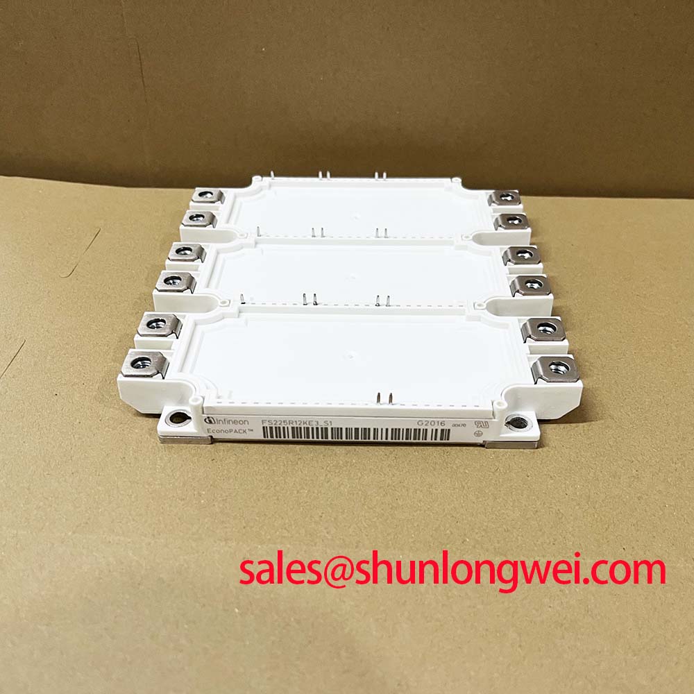
The Infineon FS225R12KE3 has the following Official Specifications: collector-emitter blocking voltage of 1200 V, nominal collector current of 225 A, and peak gate-emitter voltage of ±20 V. The current rating should not be treated as an unconditional continuous operating capability. Its specified construction is an EconoPACK™+ B package with a sixpack, three-phase inverter bridge topology and solder-pin control connections. These characteristics establish the starting point for electrical and mechanical compatibility assessment; gate-drive behavior and cooling performance remain integration tasks.
Separate the load-current emitter path from the gate-driver return on the circuit drawing, then establish which physical terminals implement those connections. The supplied package and topology specifications do not establish a dedicated Kelvin emitter terminal. Identify any auxiliary emitter connection from the model-specific terminal diagram rather than assigning that function to a convenient pin. Where a dedicated return is documented, its benefit depends on the external routing preserving that separation.
As a Design Consideration, shared emitter-path inductance can shift the driver reference during rapid current transitions. The resulting voltage disturbance changes the effective gate-emitter voltage even when the driver output appears stable relative to its own ground. Cold continuity checks help map the board connections, but they do not characterize this dynamic effect. Examine whether the driver return joins a power-current path before reaching the module, and whether neighboring commutation conductors couple into the gate loop.
For waveform assessment, reference the measurement to the appropriate local emitter connection and use probing equipment suitable for the switching potential. Long probe connections can introduce ringing that resembles an actual gate disturbance. Compare the driver output with the voltage measured at the module connection under the same switching event. Differences can identify external loop effects, although probe loading and measurement bandwidth must also be considered.
The ±20 V peak gate-emitter rating is an Official Specification, not a recommended drive amplitude. As an Engineering Recommendation, assess both positive overshoot and negative excursions at the module, including startup, shutdown, and fault turn-off. Miller-coupled current during opposite-switch commutation should be evaluated through the driver's sink path, return routing, and any implemented clamping function. Selecting a driver solely by its advertised peak output current overlooks these interacting paths.
Practical tip: Keep gate and return routing closely coupled and power commutation paths balanced, then verify the resulting gate excursions and collector-voltage overshoot with a suitably controlled double-pulse test.
Field Diagnostics & Commissioning: Common-Mode Transient Immunity in FS225R12KE3 Topologies
Correlate an unexpected gate pulse with the switching-node transition before changing the isolation component or gate resistance. A pulse seen at the controller, isolation output, and module gate represents a different fault path from one appearing only at the power-stage connection. Capture these signals with appropriate isolation and timing alignment so that propagation delay is not mistaken for noise-induced triggering.
As a Design Consideration, common-mode transient immunity belongs to the selected driver or isolator under its specified test conditions; it is not established by the FS225R12KE3 blocking-voltage rating. Reinforced insulation is likewise a system barrier requirement, not an inference from package appearance. Assess the driver's working-voltage classification, insulation documentation, transient behavior, and isolated power supply together. Board creepage and clearance should follow the applicable equipment requirements, including the actual installation environment.
When investigating simultaneous conduction, compare the actual gate transitions of complementary switches rather than relying only on programmed dead time. Driver delay mismatch, gate discharge, Miller coupling, and switching-current conditions affect the interval during which conduction can overlap. An Engineering Recommendation is to validate interlocking during enable, disable, and fault recovery as well as normal pulse operation. The timing allowance should be established from measured behavior across the intended operating conditions, not copied from another inverter.
Protection coordination requires a separate review of the semiconductor fuse, DC-link energy, and electronic shutdown path. As a Design Consideration, fuse clearing I²t describes accumulated current-squared exposure, but it cannot by itself establish IGBT survival during a hard short circuit. Available fault current, clearing characteristics, circuit inductance, and the device's applicable short-circuit limits all matter. Electronic detection and controlled turn-off address a different timescale from upstream fault disconnection; a fuse should not be treated as a substitute for gate-driver protection.
The comparison below distinguishes the established FS225R12KE3 identity from a separate sourcing candidate without implying interchangeability.
| Assessment point | FS225R12KE3 | FP100R12KT4-B11 |
|---|---|---|
| Manufacturer | Infineon | Infineon |
| Established electrical ratings | 1200 V collector-emitter; 225 A nominal collector current; ±20 V peak gate-emitter | Consult datasheet for model-specific electrical ratings, circuit diagram, and package details |
| Established physical configuration | EconoPACK™+ B; sixpack; solder-pin control connections | Requires independent footprint and connection assessment |
| Replacement decision | Match the original equipment requirements and drive conditions | Not established as a drop-in replacement |
A sourcing review involving FP100R12KT4-B11 should therefore compare circuit functions, current capability, thermal interfaces, and driver requirements before considering board changes. Industrial inverter welders and medium-frequency induction-heating power supplies are potential compatibility-assessment examples, but the complete power-conversion circuit must accommodate this module's three-phase bridge configuration. Equipment type alone does not establish suitability.
At the wider converter level, FZ400R65KF1 is a separate power-module reference requiring its own topology and rating assessment, not an assumed front-end rectifier or direct companion. Distinguish the incoming conversion stage, DC link, and inverter on the equipment schematic before associating modules with particular circuit roles. This avoids transferring specifications between electrically different stages.
Preventing Terminal Overheating: Inspection Guidelines for FS225R12KE3
Distinguish the solder-pin control interfaces from the power-terminal connections before applying maintenance rules. Solder-joint condition and conductor support are relevant inspection points for the control connections; power connections require assessment of contact condition and current distribution. A bolted-joint resistance target should not be presented as a universal FS225R12KE3 terminal acceptance limit, and a generic fastening torque does not describe its electrical pin connections.
As an Engineering Recommendation, compare thermal images under repeatable load and cooling conditions. Record the operating current, coolant or airflow condition, ambient temperature, and elapsed operating state alongside each image. An apparent hotspot can reflect surface emissivity, viewing angle, nearby heat sources, or unequal current distribution. Compare equivalent connections and follow up anomalous patterns with electrical measurements rather than assigning a cause from color alone.
A four-wire resistance measurement can help evaluate accessible conductive joints when parallel paths are understood. As a Design Consideration, test-lead placement determines which portion of the connection is included, while temperature affects comparison between measurements. Use repeatable pickup locations and compare results with an established assembly baseline or equivalent circuit position. A low reading across the whole path can conceal a localized defect if another branch carries the test current.
Mechanical support also affects the connection. Check whether board movement, conductor strain, or heatsink attachment loads are transferred into the pins. Examine soldered interfaces for changes around the joint and confirm that the assembly follows the equipment's mechanical drawing. For bolted power connections, use the applicable module and assembly instructions for contact preparation and tightening; these requirements do not apply to the module's solder pins.
The 225 A nominal collector-current specification should remain distinct from an assembly's demonstrated continuous operating capability. As a Design Consideration, semiconductor losses, heatsink performance, interface condition, and conductor heating determine the temperatures reached in service. Establish an inspection interval from equipment duty and observed trends rather than assigning a universal calendar period. For the underlying relationship between gate behavior, losses, and thermal loading, The Ultimate IGBT Knowledge Base provides supporting technical context.
FS225R12KE3 Thermal-Electrical Optimization: Antiparallel Freewheeling Diode Reverse-Recovery Tuning
Capture commutation current and collector-emitter voltage together when investigating a current spike associated with freewheeling-diode recovery. The measured peak can include load current, reverse-recovery current, and displacement current from circuit capacitance. Establish the switching sequence and measurement polarity before attributing the entire waveform to diode recovery. Recovery characteristics should be interpreted at the applicable current, temperature, and commutation conditions.
As a Design Consideration, faster turn-on can increase the severity of diode commutation and excite ringing in the surrounding power loop. Adjusting turn-on gate resistance changes this interaction but also affects switching loss and transition time. Evaluate the resulting voltage, current, and thermal behavior together rather than optimizing a single oscillogram. The FS225R12KE3's 1200 V blocking specification remains the relevant device boundary when assessing measured collector-voltage peaks.
For an RC snubber assessment, first identify the ringing path and dominant parasitic elements. An Engineering Recommendation is to place damping where it acts on the relevant loop, then assess component pulse loading, dissipation, and physical connection inductance. A remotely mounted network can leave the local oscillation largely unchanged. MOV-based overvoltage absorption, where present in the equipment, addresses a different energy and clamping problem; its voltage-current behavior and placement must coordinate with the surrounding circuit.
Technology comparisons also require care. The article on Infineon TRENCHSTOP™ IGBT7 discusses a different module generation and associated technology. Its discussion can inform questions about switching and thermal behavior, but it does not establish the FS225R12KE3's internal construction, recovery values, or operating limits. Gate settings and loss figures should not be transferred between generations on the strength of a shared manufacturer.
After each damping or gate-drive change, compare diode commutation, opposite-switch gate disturbance, and temperature rise at repeatable operating points. Record probe placement and switching conditions with the traces so subsequent comparisons remain meaningful. Resolve excessive recovery-related ringing through the identified current path, then verify the result in the assembled converter, where cabling, bus structure, and enclosure arrangement can change the observed emissions.