


Content last revised on June 1, 2026
VI-262-CU: High-Density 100W DC-DC Converter Module for Demanding Applications
A Technical Overview for Engineering Professionals
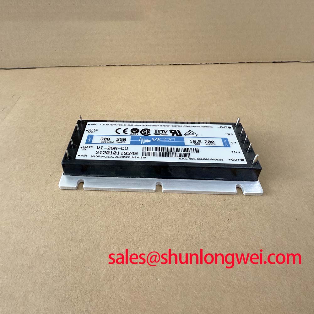
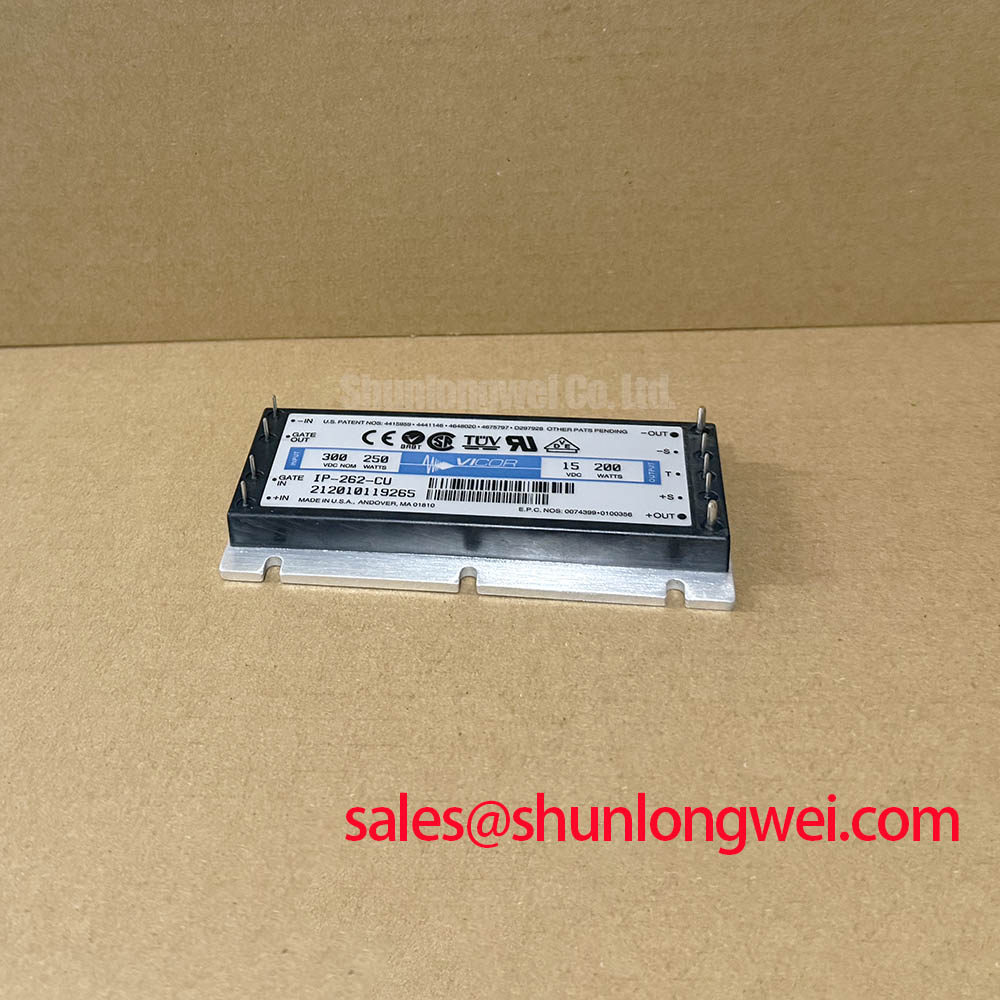
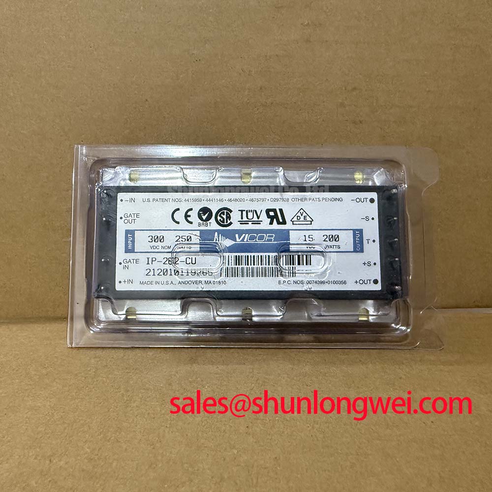
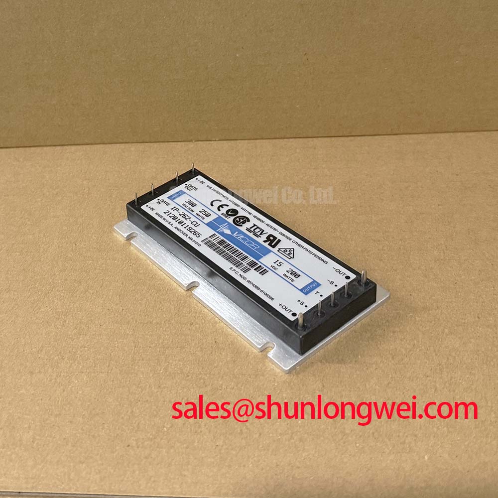
The Vicor VI-262-CU is a high-density DC-DC converter module that delivers exceptional efficiency and low noise, simplifying thermal management in space-constrained, high-reliability systems. Leveraging a proprietary zero-current switching topology, this module provides a tightly regulated 5.5V output from a wide-range DC source. Key specifications include: 300VDC Nominal Input (200-400V Range) | 5.5VDC @ 18.2A Output | 100W Power | Up to 90% Efficiency. This component offers the tangible engineering benefits of a reduced thermal footprint and enhanced power density. For systems requiring robust performance from an unregulated high-voltage DC bus, the VI-262-CU's wide input range and high efficiency make it a superior design choice.
Application Scenarios & Value
System-Level Benefits in Automated Test and Industrial Control
The best fit for the VI-262-CU is in systems where power density and low electromagnetic interference (EMI) are critical design constraints. Consider the challenge of powering sensitive analog-to-digital converter (ADC) boards within a dense Automated Test Equipment (ATE) rack. The primary engineering challenge is delivering clean, stable power without occupying excessive space or requiring bulky, complex filtering solutions that can compromise signal integrity.
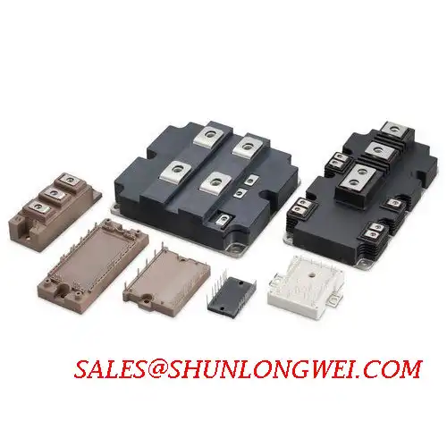
The VI-262-CU directly addresses this by integrating a high-frequency (MHz) zero-current switching (ZCS) converter. This architecture inherently produces significantly lower noise compared to conventional hard-switching converters, minimizing interference with sensitive measurement circuits. Its high power density allows designers to place the power conversion stage closer to the point-of-load, improving transient response and reducing voltage drop across long traces. This approach is fundamental to modern Distributed Power Architectures (DPA), enabling smaller, more efficient, and more reliable end systems. For the high-power AC/DC front-end that typically generates the DC bus for such distributed systems, designers often evaluate robust switching components like the SKM300GA123D IGBT module to ensure a stable high-voltage source.
Key Parameter Overview
Decoding Performance: Specifications and Their Engineering Implications
The technical specifications of the VI-262-CU are a direct reflection of its underlying technology. The following table highlights key parameters and interprets their value in a practical engineering context.
| Parameter | Value | Engineering Value & Interpretation |
|---|---|---|
| Input Voltage Range | 200 – 400 VDC (300V Nominal) | Provides significant design margin and system resilience. It ensures stable operation during line sags and swells from a PFC front-end or an unregulated DC bus, critical for reliability in industrial environments. |
| Output Power | 100 Watts | A substantial power level for its compact footprint (4.6" x 2.4" x 0.5"), enabling the powering of complex logic, processors, and auxiliary rails without consuming excessive board real estate. |
| Efficiency | Up to 90% | Directly translates to lower waste heat. An 88% efficient module generates 13.6W of heat at full load, whereas a 78% efficient one would generate 28.2W. This 50%+ reduction in heat drastically simplifies heatsink selection and thermal management. |
| Load Regulation | ±0.2% | Ensures a highly stable output voltage from no-load to full-load conditions. This is vital for powering sensitive components like FPGAs and ASICs where voltage stability is directly tied to processing accuracy and system stability. |
| Output Voltage Trim Range | -10% to +10% | Offers flexibility to compensate for voltage drops in the power distribution network (PDN) or to fine-tune the voltage for specific component requirements, simplifying system integration. |
Download the VI-262-CU datasheet for detailed specifications and performance curves.
Technical Deep Dive
Understanding the Core: Zero-Current Switching (ZCS) Technology
The standout feature of the VI-262-CU is its use of a high-frequency Zero-Current Switching (ZCS) forward converter topology. To understand its impact, it's helpful to use an analogy. A conventional "hard-switching" converter operates like a light switch being abruptly flipped on and off while current is flowing. This sudden interruption creates significant electrical noise (EMI) and thermal stress, much like the jarring "snap" and spark you might see from a high-power mechanical switch.
In contrast, ZCS is a more elegant approach. What is the primary benefit of its ZCS design? Minimized switching losses and dramatically lower EMI. It works by intelligently timing the switching event to coincide with the moment the current naturally falls to zero in a resonant circuit. Think of it like pushing a child on a swing: you apply force at the very end of the backswing, just as the motion pauses. This requires minimal effort and results in a smooth, efficient transfer of energy. By switching at the zero-current point, the VI-262-CU avoids the violent voltage and current overlaps that cause losses and noise, leading to higher efficiency and a cleaner output that requires less filtering.
Frequently Asked Questions (FAQ)
How does the zero-current switching (ZCS) topology of the VI-262-CU benefit my design beyond just efficiency?
Beyond the significant improvement in efficiency, the ZCS topology generates far less high-frequency noise (EMI). This can lead to a simpler, smaller, and lower-cost input filter design to meet regulatory standards like CISPR or FCC, saving both board space and component cost.
What is the significance of the specified power density for system-level design?
A high power density, in this case delivering 100W from a compact module, enables the overall miniaturization of the end product. It allows designers to build more powerful systems within existing mechanical enclosures or to reduce the size and weight of new designs, which is a critical advantage in portable test equipment and aerospace applications.
Can the output voltage of the VI-262-CU be adjusted?
Yes, the output voltage is trimmable from -10% to +10% of its nominal 5.5V setting. This is accomplished by connecting an external resistor between the Trim pin and either the +Sense or -Sense pin, providing valuable flexibility for fine-tuning system voltages.
What are the key considerations when paralleling multiple VI-262-CU modules for higher power?
These modules can be paralleled for higher power or redundancy. The recommended method is to use the PC pin for current sharing. By connecting the PC pins of all paralleled modules together, they can actively balance the load current between them. It is crucial to ensure identical output voltage trim settings for optimal performance. You can explore current sharing principles for more context on load balancing.
How does the wide 200-400 VDC input range impact reliability when powered from an unregulated DC bus?
An unregulated DC bus, often found in cost-effective systems or those powered by batteries, can have significant voltage fluctuations. What is the advantage of a wide input range? Enhanced system robustness. The VI-262-CU's ability to operate across this wide range without degradation in performance ensures a stable output, protecting downstream electronics and preventing system resets or failures caused by input voltage instability.
An Engineer's Perspective on Integration
From a design engineering standpoint, the VI-262-CU is more than a component; it is a solution that resolves the persistent conflict between power, space, and thermal performance. Its architecture offloads the complexity of high-frequency power design, allowing engineering teams to focus on their core application logic. The combination of high efficiency and a wide input range provides a robust power foundation, reducing the design cycles typically spent on thermal mitigation and input-side protection. This ultimately translates to a faster time-to-market and a more reliable end product.