



Content last revised on September 12, 2026
Transient Dynamics and Electrical Design for IXTN79N20
| Manufacturer | IXYS |
| Part Number | IXTN79N20 |
| Category | IGBT Module |
| Official Current Rating | 79 A |
| Package | ISOTOP / SOT-227 |
| Topology | General Power Stage |
| Voltage Rating | Not specified in the supplied official parameter set |
Capture the collector to emitter waveform and case temperature during the abnormal switching event before removing the IXTN79N20 from the power stage; this separates electrical overshoot from thermal accumulation and provides a useful comparison with a known good inverter leg.
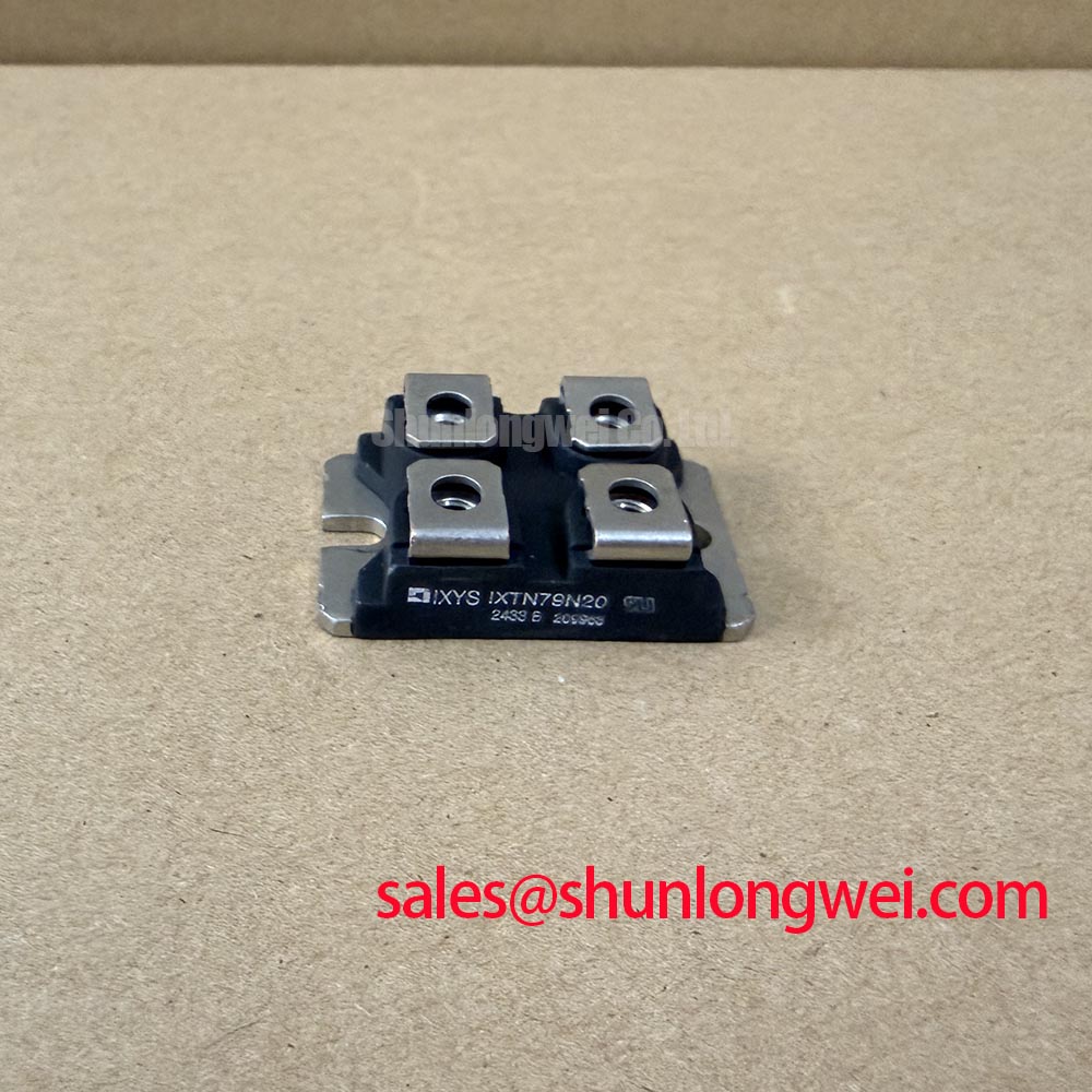
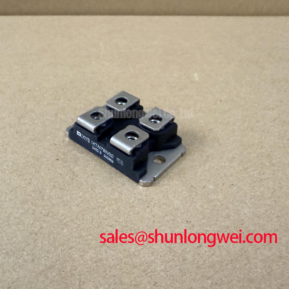
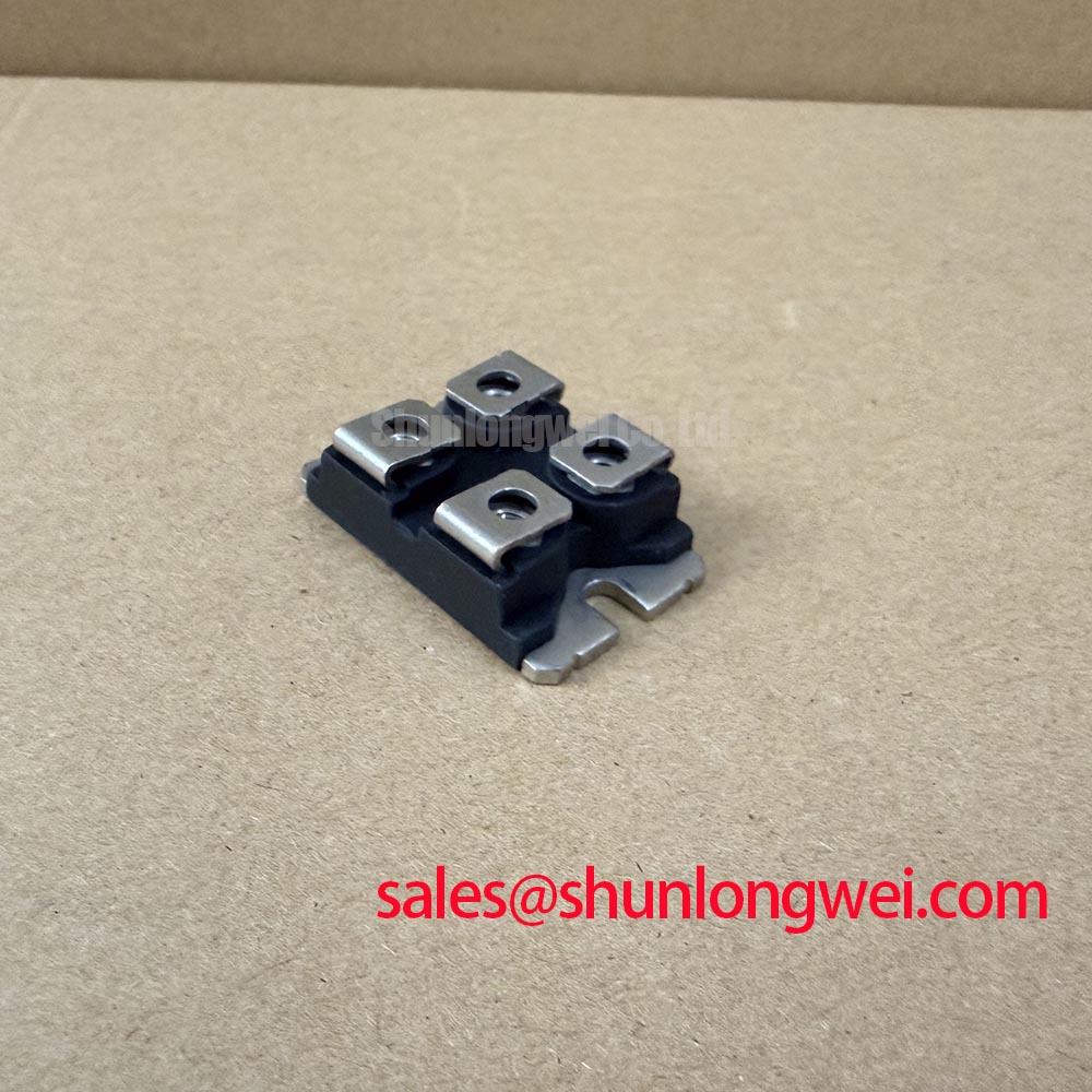
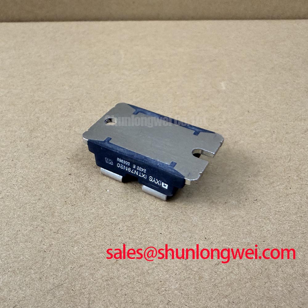
The supplied official data identifies the IXTN79N20 as an IXYS IGBT module with a 79 A current rating in an ISOTOP / SOT-227 package. The supplied parameter set does not include VCES, junction temperature limits, thermal resistance, transient thermal impedance, gate charge, switching energy, or short circuit withstand time. Those values are therefore system verification items rather than assumptions for a thermal calculation.
For a pulsed overload assessment, record the actual pulse width, repetition rate, DC bus condition, load current, switching frequency, and case temperature. A junction temperature estimate can only be made responsibly when the original thermal impedance curve and maximum junction temperature are available. A multi-RC thermal model may then be used to translate the measured case-temperature profile into a transient junction-temperature estimate. Without those manufacturer curves, a calculated peak Tj would give a false level of precision.
Long motor cables and inverter output wiring deserve particular attention. Their distributed inductance and capacitance can create reflected-wave behavior, with a remote motor terminal experiencing a voltage peak substantially above the local inverter waveform. A filter, output reactor, or suitable dv/dt network may reduce the stress, but its selection depends on cable length, motor insulation, switching edge rate, common-mode current, and the complete inverter topology. Verify the result at both the module terminals and the motor terminals rather than relying on a measurement taken only at the DC link.
Positive temperature coefficient behavior can support static current sharing when multiple devices are paralleled, but it does not by itself guarantee dynamic sharing during turn-on or turn-off. Gate-drive resistance, propagation delay, emitter path inductance, device parameter spread, and physical busbar symmetry all influence transient current distribution. Designers evaluating a multi-device arrangement should compare individual collector current waveforms and check that the hottest device remains within the verified operating boundary.
For a commercial string inverter or microgrid energy-storage converter, the IXTN79N20 should be evaluated as part of the complete switching cell. The surrounding DC-link capacitor, precharge circuit, freewheeling path, current sensor, gate driver, and protection circuit determine the stress seen by the module. A neutral comparison point for a different power-stage component is the CM800HA-28H; electrical, mechanical, and gate-drive compatibility must be checked independently rather than treating product-family similarity as a drop-in conclusion.
IXTN79N20 Operational Boundaries Under Common-Mode Transients
Probe the gate-emitter voltage directly at the module terminals while monitoring the collector-emitter waveform during the suspected false-trigger event; compare the result with the driver-side signal to identify common-mode coupling, ground bounce, or a timing fault.
No reinforced isolation rating or common-mode transient immunity specification was included in the supplied official data for the IXTN79N20. It is therefore not technically appropriate to assign a specific isolation voltage or CMTI value to this module. Isolation performance belongs to the selected gate-driver and system insulation design, while the IGBT module itself must be operated within the electrical ratings and switching conditions documented for the exact device revision.
A common-mode transient can couple through the gate-emitter capacitance, driver isolation capacitance, heatsink structure, measurement equipment, or parasitic paths around the DC-link loop. The effect may appear as a short gate pulse, an abnormal gate plateau, or a measurement artifact. Use a probe arrangement with suitable common-mode capability and a short connection between the probe reference and the actual emitter reference. A long oscilloscope ground lead can create a waveform that does not represent the module terminal voltage.
Reverse recovery in the freewheeling path can add voltage overshoot and ringing when the IGBT turns on. The correct response is not to assume a particular diode technology or recovery profile for the IXTN79N20. Instead, measure the commutation current, diode voltage, gate voltage, and switch-node waveform together. A snubber or clamp network may be considered when the measured ringing exceeds the validated system margin, but the capacitance, damping, voltage rating, and pulse-energy capability must be selected from the actual switching waveform.
Radiated and conducted interference control also depends on enclosure bonding, cable routing, shield termination, gate-driver supply decoupling, and the physical separation of control and power circuits. The external reference Field-Stop and trench-gate IGBT architecture overview provides general semiconductor background, but it should not be treated as a device-specific construction statement for this IXYS part.
Field Diagnostics and Gate-Drive Loop Commissioning
With the DC bus isolated and discharged, check gate-emitter resistance, inspect the gate connector and mounting interface, then compare the measured gate waveform against the driver output before applying a controlled low-energy switching test.
The ISOTOP / SOT-227 mechanical format places the quality of the external current-return path under the control of the system designer. The high-current emitter connection and the gate-driver return should follow the intended terminal arrangement and remain physically separated as far as the mechanical design permits. Shared copper, narrow return paths, or a gate return routed beside a high di/dt collector loop can produce emitter-voltage movement that the driver interprets as a gate signal error.
When the gate waveform shows ringing, first inspect the physical loop formed by the driver output, gate connection, emitter return, and local bypass components. Then check the driver supply at the driver pins during switching. A fault that disappears when the power stage is disabled may be caused by common-emitter inductance, inadequate local decoupling, excessive probe capacitance, or an unstable driver supply. These possibilities should be separated through waveform comparison rather than assigned to the IXTN79N20 without measurement.
Gate resistance is a tuning variable, not a universal fixed value for this module. Increasing it can slow the switching edge and reduce ringing, while reducing it can increase switching speed and associated electromagnetic stress. The final value depends on the gate-driver current capability, required switching loss, bus inductance, load current, and measured overshoot. Any change should be validated at the intended DC-link voltage and worst-case current.
Do not infer a damaged gate from a single resistance reading alone. Check the gate-emitter path, collector-emitter behavior in a safe unpowered test, the driver output, and the surrounding protection components. If the waveform differs from a reference unit, trace the signal path from the controller to the driver and then to the module terminals. The Field Engineer’s Handbook can support a broader measurement and failure-analysis workflow.
Bench Diagnostic: Disconnect power and fully discharge the DC link before connecting or removing gate-drive and power terminals.
DC-Bus Low-Inductance Layout and Thermal-Electrical Tuning
Measure the switch-node overshoot at the IXTN79N20 power terminals with a properly referenced high-voltage probe, then compare it with the DC-link voltage and the turn-off current slope to determine whether the bus structure or the snubber network requires attention.
Turn-off overshoot is governed by the interaction between stray inductance and current slew rate. In practical terms, the peak voltage rises when the commutation loop contains unnecessary inductance or when the switching edge is excessively fast for the physical layout. The useful design principle is to minimize the high-current loop area, keep the outgoing and return conductors close together, and validate the resulting peak voltage with a double-pulse or equivalent switching test.
A laminated busbar can reduce loop area by placing opposing current paths in a controlled geometry, but the actual result depends on layer spacing, terminal transitions, capacitor placement, mechanical clearances, insulation system, and connection to the module terminals. The often-quoted inductance target must not be assigned to this product without a complete mechanical drawing and field measurement. Use the system’s measured overshoot and required voltage margin to establish the acceptable layout objective.
Snubber selection should follow the observed ringing frequency, peak voltage, pulse energy, and repetition rate. A capacitor that suppresses one operating point may increase turn-on current or capacitor loss at another. Damping resistance, capacitor technology, mounting position, and thermal dissipation should therefore be evaluated together. Place the network close to the commutation terminals when the measured parasitic path shows that a remote component cannot control the local transient.
Thermal and electrical optimization must also include the mounting interface. The SOT-227 package requires a mechanically stable, electrically appropriate installation with a clean heat-transfer surface and controlled fastening practice. The heatsink, interface material, clamping method, and enclosure airflow determine the case temperature used in the thermal assessment. Confirm the manufacturer’s mechanical instructions for the exact package variant before final assembly.
The reference parasitic-capacitance overview explains how Ciss, Coss, Crss, and related coupling paths influence switching behavior in power semiconductors. For the IXTN79N20, the practical commissioning task is to measure the complete installed circuit and verify gate stability, switch-node overshoot, thermal response, and load-current sharing under the operating conditions of the commercial inverter or microgrid storage system.