

Content last revised on September 29, 2026
J2-004A-D Thermal Electrical Optimization: Thermal Feedback Practical Tuning
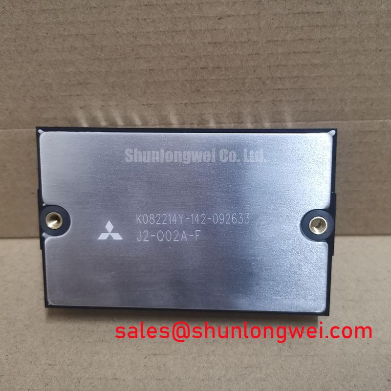
| Model | J2-004A-D |
| Manufacturer | Fuji Electric |
| Category | Power Transistor and Darlington Module |
| Rated Current | 4.0 A |
| Package | Power Transistor Module |
| Working Voltage | Standard Industrial Rating |
Measure the phase output current, case temperature, and gate signal at the same operating point when a robotic axis shows uneven heating or intermittent torque; compare each channel with a known good waveform before changing the module. The Fuji Electric J2-004A-D is specified as a 4.0 A power transistor and Darlington module, so the installed circuit must be evaluated against its original current, voltage, switching, and cooling requirements rather than inferred from package appearance.
As a Design Consideration, the positive temperature coefficient associated with VCE(sat) can support steadier static current sharing between matched parallel devices. Dynamic balance still depends on symmetrical gate loop wiring, equal conductor impedance, and consistent emitter and collector connections. Inspect the gate drive path for unequal routing, loose terminals, contamination, or damaged insulation. During testing, observe the gate to emitter waveform and collector switching node with suitable differential measurement equipment. Ringing or timing differences may indicate layout impedance, driver interaction, or measurement error and should be checked against the original signal path.
Keep the heat transfer path clean and continuous. Remove accumulated dust from the heatsink and verify that the cooling airflow reaches the complete mounting surface. Dry, high temperature cycling can age thermal interface material, while condensation can reduce insulation reliability during cold starts. ⚠️ Maintenance Note: Monitor contact temperature during scheduled maintenance and recheck airflow after cleaning or cabinet work.
For selection review, the neutral comparison point 6DI50AH-050 can be examined as another power module listing, but electrical compatibility must be established from the equipment schematic and the relevant device documentation.
Transient Dynamics and Electrical Design: Overvoltage Trip Prevention via Fast Switching on J2-004A-D
Capture the DC link and switching node together when an axis drive trips during deceleration, then correlate the overvoltage event with motor speed, braking command, and current direction. The braking transistor and ballast resistor must be selected from the actual motor kinetic energy, DC link behavior, duty cycle, and enclosure cooling capacity; the 4.0 A device rating alone does not define the complete braking circuit.
As an Engineering Recommendation, check whether the braking path absorbs energy within the limits established by the drive manufacturer and system test plan. A resistor that is electrically suitable for a short pulse may still exceed its thermal capability during repeated robotic movements. Confirm resistor temperature, braking current, and DC link recovery across the complete motion profile rather than relying on a single unloaded test.
Freewheeling diode reverse recovery can interact with wiring inductance and the gate drive, producing voltage overshoot and radiated electromagnetic interference. Review the commutation loop, diode current transition, and gate resistance during oscilloscope testing. Snubber selection should be based on measured ringing frequency, energy loss, insulation clearances, and acceptable device temperature. Industry background on alternative power switching behavior is available from Mitsubishi Electric SiC Power Modules and SBDs.
Transient Dynamics and Electrical Design: DC Link Capacitance Bank Layout and Low ESR on J2-004A-D
Probe the module terminals and the nearest DC link capacitor during turn off when the measured voltage contains a sharp spike, then compare that waveform with the controller’s DC link measurement. The practical relationship between peak voltage, DC voltage, stray inductance, and current change means that reducing the commutation loop is usually more effective than adding capacitance without layout review.
Use a compact, symmetrical bus structure so the positive and negative current paths remain close and have similar impedance. Place high frequency decoupling where it serves the switching loop, while the bulk capacitor bank handles lower frequency energy exchange. The system designer must determine capacitance, ripple current, voltage rating, damping, and thermal capability from the switching frequency and motor duty profile. Do not treat a nominal low ESR value as proof of low total loop inductance, because terminals, bus joints, capacitor leads, and mounting hardware also contribute.
Inspect busbar joints for discoloration, looseness, and uneven contact pressure. Verify creepage and clearance against the system voltage and contamination environment. If the drive uses long motor cables, test for transmission line reflection and possible double amplitude at the motor terminals; output filtering and switching edge control should be validated with the installed cable length and motor insulation system. The reference article The 1200 V CoolSiC™ MOSFET Advantage in Three provides additional context for high speed three phase conversion evaluation.
Benchtop Waveform Tuning: Mitigating Stress via Thermal Time Constants and Peak Junction Temperature
Record collector current, case temperature, pulse duration, and switching waveform together when the module runs correctly at low load but becomes unstable during repeated acceleration or braking. Use the device’s published transient thermal impedance data, when available, to build the junction to case response for the actual pulse pattern; do not estimate peak junction temperature from steady state case temperature alone.
A multi RC thermal model is an Engineering Calculation tool for separating short pulse heating from longer case and heatsink response. The model should include interface condition, heatsink airflow, mounting pressure, ambient temperature, and pulse repetition. Its result must be checked with measured case temperature and electrical stress waveforms, because thermal interface aging and cabinet airflow can shift the practical result.
During bench tuning, increase operating stress gradually while watching desaturation or overcurrent protection behavior, gate waveform stability, and collector overshoot. If a thermal rise appears only after several motion cycles, compare the accumulated energy with the cooling system’s time response and inspect the heatsink for blocked fins or uneven contact. High altitude, cosmic ray effects, single event burnout, FIT values, and insulation life require application specific source data and should not be assigned as fixed properties of this module without authoritative documentation.