Content last revised on October 17, 2026
Benchtop Waveform Tuning: Thermal Management and Switching Stress in MCD312-12IO1
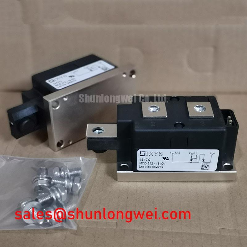
When a high current power stage reports a thermal or conduction fault, isolate the supply, inspect the copper baseplate contact, and compare the cold terminal condition with the known circuit topology before applying another test pulse. The device identified for this evaluation is the IXYS MCD312-12IO1, a thyristor/diode module with a specified blocking voltage of 1200.0 V and a TO-240AA housing. Its current capability must be assessed using the datasheet’s separate average and RMS ratings and their specified thermal conditions.
These ratings define the component identity, not the complete operating limit of an assembled converter. A medium-frequency induction melting or hardening power supply can expose the module to repetitive thermal cycling, line transients, commutation stress, and uneven current sharing. The original gate and power terminal arrangement, semiconductor fuse coordination, heat sink condition, and switching waveform should therefore be checked as one working assembly.
| Manufacturer | IXYS |
| Part number | MCD312-12IO1 |
| Device category | Thyristor/Diode Module |
| Specified blocking voltage | 1200.0 V |
| Current ratings | Refer to the datasheet for average and RMS ratings under the specified conditions |
| Package | TO-240AA |
Thermal evaluation should begin at the junction-to-case path, with the copper baseplate seated evenly against a clean, flat heat sink. Check the contact pattern after removal rather than relying only on visual inspection: an interrupted paste imprint or a concentrated edge mark can indicate uneven pressure, baseplate distortion, or a mounting surface that is not supporting the full module footprint.
The relevant thermal resistance is the datasheet-defined Rth(j-c) value, which should be used with the actual conduction pattern, duty cycle, ambient conditions, and heat sink performance. It is not appropriate to substitute a generic module value for the MCD312-12IO1. Apply the thermal interface material as a thin, continuous layer suitable for the mounting surface, then tighten the fasteners in a controlled sequence using the manufacturer’s specified mounting torque. Excessive force can distort the baseplate and reduce the uniformity that the thermal path depends on.
During waveform tuning, observe the voltage across the power terminals and the gate response at the module terminals. Gate wiring should remain short and physically separated from high di/dt power paths. When several thyristors operate in parallel, the driver and conductor geometry should be matched so that turn-on delay and gate current do not create avoidable dynamic current imbalance. Static current sharing must also be verified across the operating temperature and current range; it should not be assumed from temperature coefficient behavior alone.
The semiconductor fuse selection must be matched to the device’s surge-current and I2t withstand data. Compare the fuse’s total clearing I2t and clearing characteristics with the module’s applicable withstand limits and the protection requirement of the complete converter. A module current rating should not be treated as a fuse sizing instruction.
Assembly Integrity & Layout Architecture: Applying IEC 61000-4-5 Surge Immunity Testing to Systems Using MCD312-12IO1
Surge protection begins upstream of the thyristor junctions, where the AC input network, semiconductor fuses, MOV arrangement, wiring inductance, and RC snubber stage must be considered together. The purpose of the protection network is to limit the transient energy reaching the module while preserving the intended commutation and gate-trigger behavior.
For an induction heating power supply, place surge-limiting components according to the cabinet topology and the physical path from the incoming terminals to the power bridge. MOV selection should account for the system’s steady-state voltage, temporary overvoltage conditions, expected surge class, and available short-circuit energy. The surge test level and installation method should be assessed against the applicable IEC 61000-4-5 test framework rather than inferred from the module’s 1200.0 V rating.
RC snubbers can reduce excessive dv/dt and ringing, but their values are system-dependent. Select and validate them from measured commutation waveforms, capacitor pulse capability, resistor energy, and the actual parasitic layout. The TT92N14KOF device may be evaluated as a neutral reference for a related rectifier stage, but electrical compatibility must be established from topology, voltage, current, gate requirements, and thermal conditions rather than package appearance.
💡 Pro Tip: Keep the high-current forward and return paths physically symmetrical, then verify overshoot and ringing with an appropriately rated differential probe during controlled switching tests.
Field Diagnostics & Commissioning: Short-Circuit Withstand Limits and Coordination in MCD312-12IO1 Topologies
A dead-short investigation should concentrate on the clearing sequence: fault current path, semiconductor fuse response, module terminal condition, and the energy absorbed before isolation. Compare the selected fuse’s total clearing I2t with the applicable thyristor and diode withstand data for the exact operating condition. The check must include prospective fault current, source impedance, fuse pre-arcing behavior, and the physical length of the fault loop.
After an interrupted fault, inspect the main terminals for movement, heat discoloration, and evidence of loosened clamping. Check the gate circuit separately from the power circuit, including gate-to-cathode continuity, driver isolation, and trigger timing. A damaged gate path may coexist with an apparently intact power path, while a power short may also result from an external commutation or snubber fault.
For systems that combine a rectifier, inverter, regenerative braking chopper, or high-power braking resistor, commissioning should separate each energy path before full-load operation. The MCD312-12IO1 should be evaluated within the original trigger sequence and commutation arrangement, including any interlock logic used to prevent unintended conduction. Removing the gate signal does not turn off a conducting conventional thyristor; its current must fall below the holding current, with sufficient recovery time before forward voltage is reapplied. Gate-loop inductance, driver return placement, and pulse buffering are layout decisions that require measurement at the module terminals.
The reference article Evolution of Negative Off-Bias Gate Drive Circuits discusses off-state gate control, but gate turn-off techniques for devices such as IGBTs should not be applied directly to this conventional thyristor module. Broadcom optically isolated amplifiers and modulators can support isolated measurement and feedback architecture reviews. Thermal test interpretation should also be separated from electrical switching results; the JEDEC JESD51 thermal test method is a suitable standards reference for understanding thermal characterization practices.