

Content last revised on September 12, 2026
MG100J2YS50 Thermal-Electrical Optimization: High dv/dt Cross-Conduction Shoot-Through Practical Tuning
Begin troubleshooting with the converter isolated from the supply and its stored energy safely discharged. Examine the gate-drive wiring as a signal path rather than treating it as a simple on and off connection. In a switching bridge, a rapid collector voltage transition can couple through device capacitances and surrounding layout into the gate loop of the opposite switch. If that unwanted gate movement reaches the switching threshold during a commutation event, simultaneous conduction can occur. The resulting current rise is often brief, yet it can impose substantial stress on the switching devices, DC-link capacitors, busbars, and protection fuse.
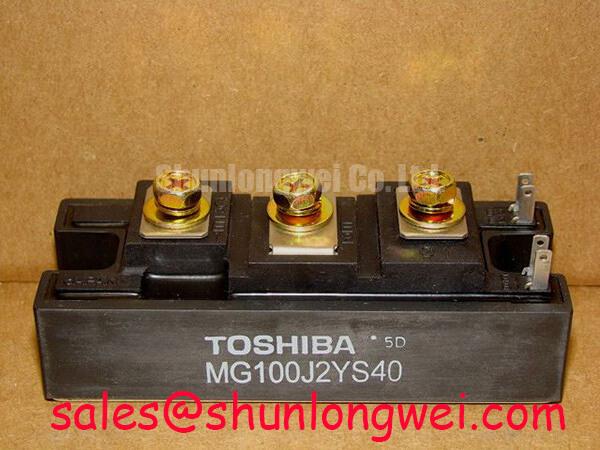
For the MG100J2YS50, the published identity data confirms the 1200 V and 100 A rating boundary, but it does not define an approved gate voltage, gate resistance, switching frequency, active-clamp setting, or negative-bias value. Therefore, a negative gate bias range sometimes discussed in general IGBT-drive practice must not be presented as a Toshiba requirement for this model. Treat low-impedance active Miller clamping and negative gate bias as a Design Consideration: they require confirmation against the actual gate-driver design and verified waveform measurements.
At the bench, capture gate-to-emitter voltage and collector-to-emitter voltage with measurement equipment suitable for the converter’s voltage and transient environment. Compare the switching event with a known-good channel where available. A gate waveform that rises unexpectedly during the companion device transition may indicate coupling through a shared return, excessive driver impedance, unsuitable probe connection, or a protection circuit that is not behaving as intended. It does not establish a single cause by itself. Check driver supply stability, gate-loop routing, gate clamp operation, and the physical condition of small driver-board components before changing values.
Keep the power commutation loop compact to reduce parasitic inductance that can intensify turn-off overshoot. This is an Engineering Recommendation, not an official MG100J2YS50 layout specification. Where a MOV and RC or other suppression network is already part of the original equipment, inspect its connections and confirm that its service condition remains appropriate to the measured transient behavior. Protection components should be evaluated as a coordinated network with the DC-link and switching waveform, not independently selected from a nominal module voltage rating.
Bootstrap circuits also deserve attention in bridge arrangements where they are used by the existing driver architecture. Their capacitor recharge path, diode recovery behavior, duty cycle, and switching rate can affect high-side drive availability. Verify the actual driver supply waveform under the equipment’s intended operating conditions. Do not assume that the module itself specifies a bootstrap component value or charging margin.
MG100J2YS50 Circuit Protection & Reliability: Calibrating Galvanic Gate Drive Isolation, Reinforced
Trace every control connection from the gate-driver board to the installed module before reconnecting power. The terminal functions and pin arrangement must be verified from the original equipment documentation or the applicable Toshiba documentation; the available official identification data does not provide a pinout. A connector can appear mechanically compatible while its control return or terminal order differs from the circuit being repaired.
Reinforced galvanic isolation, insulation coordination, and common-mode transient immunity belong primarily to the selected driver, isolator, power supply, PCB, and mechanical spacing system. They are not standalone certified properties established by the module’s 1200 V rating. As a Design Consideration, maintenance personnel should inspect the driver board for contamination, conductive dust, moisture residue, cracked coating, damaged isolation slots, and compromised creepage or clearance paths. Engineers should validate the isolation barrier and transient performance against the applicable equipment safety requirements and the driver manufacturer’s documentation.
In vibration-prone welding and induction-heating cabinets, busbar fastening should be checked with the equipment manufacturer’s assembly requirement. A loose connection can add contact resistance and create localized heat, while an over-tightened connection can damage hardware or distort a mounting interface. Confirm that phase connections, DC terminals, current-sensor paths, and auxiliary control wiring remain mechanically supported and cannot rub against sharp conductive edges.
⚠️ Maintenance Note: Periodically monitor terminal and heatsink contact temperature rise under controlled load, then clean the cooling path and recheck fastener security only with the system de-energized.
Short-circuit and fault-clearing behavior is a system-level matter. Semiconductor fuses, current sensors, driver desaturation functions, contactors, and controller response must act together within conditions defined by the original design. Fuse selection based solely on the module’s rated current is not sufficient because fault energy depends on the entire DC source, bus structure, switching state, and clearing sequence. When a fuse has operated, inspect the surrounding gate-driver and DC-link sections rather than assuming the fault originated in one component.
Equipment that also includes a human-machine interface should maintain separate documentation paths for its display and power sections. Information published by Truly industrial display modules can help identify industrial display considerations, but it is not a source for MG100J2YS50 power-module ratings or gate-drive limits.
Transient Dynamics & Electrical Design: Auxiliary Emitter Return Trace Separation on MG100J2YS50
When examining an existing power stage, distinguish between the high-current emitter return and any low-level gate-drive return identified by the actual module and equipment documentation. Shared inductance in a common return can convert changing load current into an unwanted voltage seen by the driver. This can alter apparent gate voltage during switching, encourage ringing, or interfere with the intended turn-on and turn-off sequence.
Use a Design Consideration of separating the low-level driver return from the main high-current emitter path where the original topology supports it. The objective is to give the driver a cleaner voltage reference while the power loop carries changing current. The exact routing, connector use, terminal allocation, and allowable loop geometry are system-determined and must be validated from the original design. Do not infer that this Toshiba module includes a particular auxiliary-emitter or Kelvin terminal without the relevant official pinout.
Oscilloscope findings should be interpreted carefully. Ringing observed at the gate can result from the real switching circuit, a ground lead placed in a noisy position, an unsuitable probe bandwidth, an unstable driver supply, or a wiring change introduced during repair. Use consistent probing methods, inspect the same operating transition repeatedly, and compare channels before modifying the gate network. Where a driver resistor or clamp component has been changed previously, return the diagnosis to documented circuit values rather than fitting an arbitrary replacement value.
Parallel-device arrangements require equal attention to static and dynamic current sharing. Temperature-dependent behavior may influence sharing, but it does not guarantee balanced current in a practical converter. Matching connection resistance, comparable thermal paths, synchronized gate-drive paths, and verified switching waveforms are Engineering Recommendations for an existing parallel design. Engineers should test current distribution and peak electrical stress within the actual equipment rather than assume equal sharing from nominally identical module markings.
For an alternative Toshiba-family reference during an engineering compatibility review, the MG100Q1ZS40 should be evaluated against the original schematic, terminal arrangement, voltage class, current requirement, driver behavior, mechanical interface, and thermal system. It is a reference point for documentation review, not a declared substitute for MG100J2YS50.
Benchtop Waveform Tuning: Mitigating Stress via Baseplate Convexity Compensation and Screw on MG100J2YS50
Before placing the module on the heatsink, clean both mating surfaces using a process compatible with the equipment’s maintenance procedure. Check for embedded debris, scratches, dried thermal compound, corrosion, and uneven residue. A clean visual inspection can reveal conditions that prevent close contact long before a power test is attempted. Inspect the heatsink for flatness concerns or mechanical damage, particularly after a cabinet impact, fan failure, or repeated high-temperature service.
Thermal interface material thickness is a Design Consideration determined by the compound, surface condition, mounting arrangement, and equipment documentation. A thin, continuous layer is generally intended to fill microscopic surface irregularities rather than create a thick insulating layer. Apply the specified material using the original manufacturer’s service procedure when available, then seat the module without sliding it excessively across the heatsink. If baseplate curvature or heatsink flatness is suspected, resolve that mechanical condition instead of compensating with an uncontrolled amount of thermal compound.
Use a gradual, alternating screw-tightening sequence so clamping force develops evenly across the module base. The proper screw size, torque, washer arrangement, thread engagement, and tightening sequence are installation-specific unless confirmed by official module and equipment documents. They must not be invented from the 1200 V, 100 A electrical rating. After assembly, verify that busbars do not apply lateral force to the module terminals and that the enclosure’s airflow path remains unobstructed.
During controlled recommissioning, inspect fan operation, filter cleanliness, air direction, heatsink contamination, and signs of condensation exposure. In environments subject to high humidity or temperature cycling, maintenance teams should examine cabinets for water ingress and ensure that the equipment’s prescribed anti-condensation measures remain functional. For broader context on changing power-semiconductor design approaches, see the Wide Bandgap Revolution technical guide; its discussion does not alter the Toshiba MG100J2YS50 official ratings or installation requirements.