Content last revised on October 11, 2026
Benchtop Waveform Tuning: Mitigating Stress via Unpowered Bench Screening with the MG300Q1UK1
- Isolate the drive, discharge the DC link, and record the module terminal identification before testing.
- Use a digital multimeter diode mode for cold checks across the main conduction paths and the documented antiparallel diode path.
- Inspect the baseplate, heatsink contact area, driver isolation barrier, and gate wiring before applying control power.
- Confirm the replacement envelope against the existing heavy-duty variable frequency AC motor drive assembly.
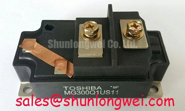
The Toshiba MG300Q1UK1 is an IGBT module rated at 600.0 V and 300.0 A, supplied in a Toshiba module package. These are official product specifications for identification and procurement. The voltage and current ratings do not, by themselves, define the allowable switching frequency, thermal operating point, short-circuit capability, or complete inverter output rating. Those limits remain dependent on the drive topology, gate-drive circuit, cooling path, protection settings, and operating duty.
| Parameter | Specification | Classification |
|---|---|---|
| Manufacturer | Toshiba | Official product identification |
| Part number | MG300Q1UK1 | Official product identification |
| Rated voltage | 600.0 V | Official Datasheet Specification |
| Rated current | 300.0 A | Official Datasheet Specification |
| Package | Toshiba Module | Official product specification |
Cold diode-mode screening should be completed before any DC-link energization or gate-drive connection. Keep the module electrically isolated from the inverter bus, motor cable, braking network, and snubber components. A clean bench test prevents surrounding circuit paths from masking the electrical condition of the power terminals.
Start by identifying the collector, emitter, gate, and auxiliary connections from the equipment drawing and the module documentation. Measure the main conduction paths in both meter polarities, then check the documented freewheel or antiparallel diode path in the forward direction. The reading should be interpreted as a comparison against a known-good module or the original maintenance record rather than as an invented universal pass or fail threshold. An unexpected open circuit, near-short reading, or strong asymmetry between corresponding paths deserves isolation testing before replacement approval.
Gate leakage screening is equally important. Keep the gate terminal disconnected from the driver output, discharge the gate-to-emitter path with an approved bench method, and check whether the meter indication remains stable when the probes are removed and reapplied. A gate reading that changes substantially with probe position, body contact, or nearby wiring may reflect a contaminated surface, an unintentional measurement path, or damage in the gate structure. The result should be compared with the same measurement on the removed reference part whenever that part is safe to handle.
For waveform work, do not connect the module to a live DC bus simply to discover whether the driver is correctly phased. Use a current-limited, isolated bench arrangement and confirm the driver output with the power stage disabled. Check that the command polarity, complementary timing, and gate reference are correct before connecting the gate terminals. The gate loop should be short, physically separated from high-current commutation conductors, and routed according to the original drive layout wherever possible.
When a replacement is being considered for a legacy board, the linked MG30G6EL2 may be evaluated as a related device in the same maintenance decision process. It should not be treated as an automatic substitute. Engineers should compare terminal assignment, electrical ratings, thermal interface geometry, gate-drive requirements, protection response, and the mechanical mounting pattern before authorizing a change.
Preventing Spurious Faults: Isolated DC-DC Power Supply Sizing for High-Immunity Gate Drive Systems
Gate-drive power integrity controls whether the MG300Q1UK1 receives a clean switching command or an unintended pulse during high-voltage transitions. The isolated DC-DC supply, driver, return path, and gate resistor form one switching interface; evaluating only the power module can miss a common-mode disturbance generated elsewhere in the inverter.
For a high-voltage industrial drive, the selected isolated gate-driver power architecture should be checked for a reinforced galvanic isolation barrier rated above 5 kV where that level is required by the system insulation plan. Common-mode transient immunity above 100 kV/µs may also be used as a system selection criterion when the switching layout produces severe voltage movement. These values are Design Considerations for the driver and isolation system, not official electrical ratings of the Toshiba module.
Review the isolation capacitance, creepage and clearance, control-side grounding, and the physical route between the isolated supply and gate driver. High-current collector and emitter paths should not share the return route used by the driver supply decoupling loop. The driver output loop should return directly to the appropriate emitter reference, with the gate resistor positioned to control the local current path. The design team should validate the actual barrier performance and transient immunity against the selected driver documentation.
Dead-time must be treated as a timing margin within the complete switching system. Propagation delay, driver asymmetry, gate charge variation, temperature, and turn-off behavior all influence the interval between complementary commands. Excessively short dead-time can permit cross-conduction, while excessive dead-time can increase diode conduction and switching stress. Set the initial value from the drive manufacturer’s timing architecture, then verify both gate waveforms and collector-emitter behavior under controlled switching tests.
TI provides a useful industry reference for isolated driver selection and common-mode behavior in isolated gate drivers for IGBT and SiC systems. This external reference can support driver architecture review, but it does not replace the Toshiba module documentation or the original inverter manufacturer’s timing requirements.
When the module forms part of a rectifier, DC-link, inverter, and braking chain, inspect the surrounding topology rather than replacing the power switch in isolation. The MG150Q2YS51 can be reviewed as a related front-end or complementary-stage device, subject to voltage class, current sharing, control strategy, and mechanical compatibility. The system integrator should confirm the required supply voltage from the original drive documentation instead of assuming a universal gate-drive value.
Assembly Integrity and Layout Architecture: Implementing Baseplate Convexity Inspection for the MG300Q1UK1
Thermal assembly quality begins with the contact surfaces, not with the control software. Before mounting the module, clean the heatsink face and inspect it for burrs, embedded debris, corrosion, or local distortion. The module baseplate should be checked for visible damage and assessed against the equipment manufacturer’s allowable flatness and convexity limits. A mechanical mismatch can create localized thermal concentration even when the mounting screws appear tight.
Apply the thermal interface material as a controlled, even layer suitable for the selected module and heatsink surfaces. The proposed 50–80 µm interface thickness is a general Design Consideration for controlled TIM application, not an official MG300Q1UK1 specification. The correct thickness depends on surface finish, interface material properties, pressure distribution, and the manufacturer’s assembly instructions. Excess material can increase thermal resistance, while insufficient coverage can leave air pockets.
Use the prescribed fastener type and tighten progressively in a diagonal cross-pattern. A calibrated torque tool is preferable to hand estimation, and the final value must follow the equipment or component assembly documentation. For a general M5 mounting reference, 2.5–3.5 N·m is a Design Consideration only, not a confirmed MG300Q1UK1 factory requirement.
Spring washers or disc-spring hardware can help maintain contact force through thermal cycling, but the stack height, spring rate, fastener length, and heatsink structure must be assessed together. Excessive pressure can distort the baseplate or substrate; insufficient pressure can allow interface movement and rising thermal resistance. Double-sided cooling arrangements require special attention to parallelism because tightening one side can alter contact pressure on the other.
After installation, inspect the terminal lugs and busbar joints for alignment before tightening electrical connections. Do not use the power terminal to pull a misaligned busbar into position. The copper connection should approach the terminal naturally, with the insulation barriers and creepage paths preserved. Keep high-current conductors compact while maintaining the clearance required by the drive’s insulation design.
🔧 Maintenance Note: Record thermal contact temperature during scheduled service and clean the heatsink and fan path before rising temperature is mistaken for semiconductor failure.
In humid or seasonally cold facilities, examine the enclosure for condensation, blocked drains, and inactive anti-condensation heating where fitted by the equipment builder. Moisture contamination around the gate terminals and control board can produce intermittent behavior that is not visible during a short dry-bench inspection.
Benchtop Waveform Tuning: Balancing Switching Dissipation and di/dt on the MG300Q1UK1
Retrofitting an IGBT module into a legacy variable frequency drive requires gate-resistor tuning around the existing driver capability, bus layout, load current, and protection response. The external turn-on and turn-off resistors should be considered as part of the complete gate loop rather than as isolated accessories. Their values influence switching transition speed, ringing, diode recovery interaction, and switching dissipation.
A practical tuning sequence starts with a low-energy, current-limited test. Capture the gate-emitter waveform at the module terminals using a measurement method suited to the switching environment, then observe the collector-emitter transition and the associated current path. Probe placement matters: a long ground lead can create ringing that is not present in the actual gate loop. Compare the waveform with the original board configuration and check whether the driver output remains within its intended voltage and current capability.
Increasing the turn-on resistance generally slows the gate-current rise and can reduce overshoot or ringing, but it may increase switching loss. Reducing it can shorten the transition while increasing di/dt stress and sensitivity to stray inductance. Turn-off resistance requires a separate assessment because rapid turn-off can increase voltage overshoot when commutation inductance is significant. The correct balance is system-determined and should be verified by measuring peak voltage, switching current, temperature rise, and fault behavior under the intended operating conditions.
Freewheel-diode reverse recovery also affects the observed waveform. Recovery softness, loop inductance, busbar geometry, and gate timing can combine to increase electromagnetic emission or voltage stress. Do not assign a specific reverse-recovery softness factor to the MG300Q1UK1 without the corresponding manufacturer data. Instead, review the complete commutation path and measure the switching node with an appropriate high-voltage differential probe.
Regenerative braking adds another operating condition. During deceleration, the DC-link energy may be directed toward a braking chopper and resistor, depending on the drive architecture. The chopper switching device, resistor thermal capacity, bus-voltage control, and fault threshold must be evaluated as a coordinated subsystem. The 600.0 V official voltage rating of the module is an identification boundary; it is not a complete braking-resistor energy specification.
Gate-trigger behavior should also be checked during repeated command pulses, especially where the legacy control board uses pulse trains, optocouplers, or long control wiring. Confirm that the driver output remains stable during common-mode transitions and that complementary devices cannot receive overlapping commands. The engineering reference IGBT Design and Integration provides additional context for gate-drive layout, thermal management, and switching topology review.
For a heavy-duty variable frequency AC motor drive, final acceptance should combine cold electrical screening, isolated gate-drive verification, controlled thermal assembly, and waveform measurement. This approach gives maintenance engineers a traceable basis for deciding whether the Toshiba MG300Q1UK1 is compatible with the existing power stage and its operating envelope.