

Content last revised on October 9, 2026
Field Diagnostics and Commissioning for Terminal Contact Stability
| Manufacturer | Toshiba |
| Product Category | IGBT Module |
| Model | MG300Q2YS45 |
| Rated Voltage | 1200.0 V Official Specification |
| Rated Current | 300.0 A Official Specification |
| Package | Toshiba Module |
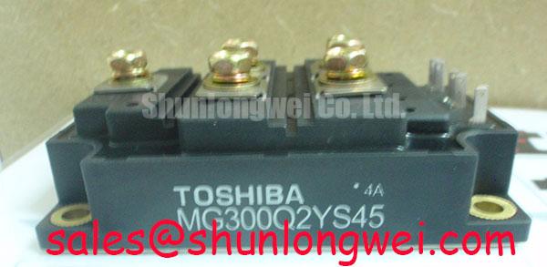
Measure the resistance of each bolted power terminal with a calibrated micro-ohmmeter before commissioning the MG300Q2YS45; a clean, mechanically stable joint is essential when a Toshiba module with a specified current rating of 300.0 A is installed in a heavy-duty variable frequency AC motor drive.
For this inspection, isolate the drive from every energy source, allow the DC-link section to discharge according to the equipment service procedure, and remove parallel current paths that could distort the reading. Probe directly across the bolted interface rather than across a long cable section. A low and repeatable contact-resistance result may be used as the inspection focus for this installation procedure, but the maintenance team should also compare readings between equivalent terminals and against the original commissioning record.
Contact resistance is only one part of the assessment. Oxidation, uneven clamping, contaminated mating surfaces, or a cable lug that does not sit flat can create a local heating point even when the module’s semiconductor ratings are suitable for the drive. Inspect the terminal faces, busbar alignment, lug condition, washer arrangement, and the mechanical support around the connection. Do not allow the busbar to pull the module terminal sideways during tightening because mechanical stress can be transferred into the package.
After the joint has been reassembled, use thermographic imaging during a controlled operating test. Compare the temperature profile of equivalent phase terminals under comparable load rather than judging one isolated image. A warmer terminal may indicate contact imbalance, cable asymmetry, airflow disturbance, or a measurement-angle issue. Confirm the observation with a second measurement method before removing the module from service.
Clearance around the power terminals should permit the correct probe placement, visual inspection, and thermal imaging without forcing the wiring into a sharp bend. Keep control wiring separated from high-current switching paths where the cabinet layout allows it. This arrangement reduces the chance that probe leads, gate wiring, or feedback cables will be disturbed during future terminal maintenance.
For equipment using direct torque control, switching behavior and current regulation are closely connected to the drive topology and control implementation. Engineers evaluating the module in that environment can consult the external reference on Direct Torque Control for high-dynamic industrial induction motor drives while checking the actual gate-drive and protection design of the equipment.
⚠️ Maintenance Note: Monitor terminal temperature trends after service and keep the heat-sink airflow path clear of accumulated dust.
Benchtop Waveform Tuning and Pre-Installation Junction Health Check
Before applying DC-link voltage, screen the unpowered MG300Q2YS45 on a controlled bench using the diode-check function of a digital multimeter, while treating the result as a comparative health check rather than a substitute for the manufacturer’s complete electrical test procedure.
Measure across the main power terminals in both polarities and compare the observed semiconductor junction behavior with a known-good module of the same type and test arrangement. The antiparallel diode should be included in this comparison because its forward path can influence the reading. Lead polarity, meter current, attached snubbers, and parallel circuit paths all affect the displayed value, so record the test setup with the result.
Gate leakage screening should be performed with the power terminals unenergized and the gate terminal referenced exactly as specified by the drive’s service documentation. Look for an unexpected low-impedance path between gate and emitter, intermittent readings caused by probe movement, or a change after the module has been handled. A leakage observation should be confirmed after cleaning the terminals and repeating the measurement with controlled polarity.
The high-side gate supply deserves separate attention when a bootstrap arrangement is used. The bootstrap capacitor must provide the required gate-charge energy for the selected switching interval while also covering driver quiescent current, charging losses, leakage, temperature effects, and the voltage drop of the bootstrap charging path. Its suitability is therefore determined by the driver, switching frequency, duty cycle, gate-charge requirement, and allowable gate-supply ripple as a complete system.
Do not select the capacitor from capacitance alone. Check the capacitor’s voltage rating, temperature behavior, dielectric characteristics, ripple-current capability, and placement inductance. The charging diode and its recovery behavior also affect the high-side supply. A slow or poorly coordinated recovery event can disturb the bootstrap node and introduce unwanted gate-voltage movement during commutation.
During the first powered waveform test, observe the gate-to-emitter voltage at the module terminals rather than at the driver board only. A long measurement ground lead can introduce ringing that does not exist at the device, while a poorly routed gate loop can create genuine common-mode ground-bounce. Use a suitable differential measurement method and keep the probe loop physically compact.
Gate turn-off behavior should be checked under the actual isolation and return-current arrangement. A negative gate bias can improve immunity to unintended turn-on in some system designs, but its value, timing, and insulation requirements are determined by the driver architecture and the module’s applicable electrical limits. It should not be added as a generic modification without checking the original drive board, gate-emitter rating, and protection coordination.
When a heavy-duty variable frequency AC motor drive is retrofitted, compare the bench waveform with the legacy board’s timing, dead time, gate amplitude, and desaturation or overcurrent response. A module with specified voltage and current ratings of 1200.0 V and 300.0 A still depends on the surrounding driver and commutation network for safe switching. Validate the complete switching loop with controlled current and voltage measurements before returning the drive to production service.
Operational Boundaries and Gate-Drive Resistance Calibration
Adjust external RG(on) and RG(off) only after the replacement module has been checked against the legacy driver’s output capability, gate-loop layout, protection timing, and switching waveform. These resistors influence the compromise between switching loss, voltage overshoot, current slew rate, and ringing; they are system-tuning elements rather than fixed product specifications for the MG300Q2YS45.
Begin with the resistor arrangement used by the original drive board if its topology is known, then inspect whether separate turn-on and turn-off paths are present. A shared resistor may produce acceptable behavior in one operating condition but insufficient control in another. Diodes, ferrite elements, clamp networks, and driver output resistance also contribute to the effective gate impedance, so the external resistor marking alone does not describe the complete gate path.
Use a controlled switching test to observe gate-to-emitter voltage, collector-emitter voltage, collector current, and the behavior of any active clamp or overvoltage network. The objective is to suppress parasitic ringing and inductive overshoot while keeping switching losses within the thermal capability of the assembled drive. The final setting should be established from measured waveforms at the module terminals, not copied from a different package or a different gate driver.
A metal-oxide varistor may be used as part of a broader overvoltage protection network, but its clamping behavior, energy rating, aging characteristics, and coordination with snubbers or active clamps must be evaluated at the system level. The MOV does not replace appropriate DC-link layout, local commutation control, or verification of the peak voltage appearing across the IGBT during switching.
For parallel devices, positive temperature characteristics can support static current sharing in suitable operating regions, but dynamic sharing remains dependent on gate-loop symmetry, emitter path inductance, switching timing, thermal coupling, and the physical busbar arrangement. When several modules are considered for a common converter leg, match the electrical path lengths and measure current distribution during turn-on and turn-off. Do not infer dynamic balance from steady-state current alone.
High-altitude installations require a separate insulation and cooling review. Reduced air density can affect external clearances, cooling performance, and the cabinet’s thermal margin. Cosmic-ray or single-event breakdown behavior may also be relevant to high-voltage power electronics, but a product page should not assign FIT values, lifetime hours, or SEB limits without an authoritative device-specific source. The responsible engineering action is to review the system’s altitude, switching voltage, transient profile, insulation coordination, and manufacturer qualification data together.
For topology-level design context, the engineering guide Peak Efficiency in Solar and Energy Storage provides a useful reference point for evaluating switching paths, voltage distribution, and protection coordination. It should be read alongside the actual converter schematic rather than used as a substitute for the drive manufacturer’s design records.
When comparing an alternative Toshiba module for a lower-current application, engineers may place MG200Q2YS1 beside the MG300Q2YS45 during a documented electrical and mechanical compatibility review. Voltage class, current requirement, terminal arrangement, gate characteristics, thermal interface, protection behavior, and control-board compatibility must all be checked before any substitution decision.
After calibration, repeat the thermal inspection at representative load conditions and record the gate waveform, switching-node overshoot, current sharing, and heat-sink temperature. A serviceable result is one that remains within the verified electrical and thermal boundaries of the complete drive, with the module, busbar, driver, protection network, and cooling assembly assessed as one operating system.