Content last revised on October 5, 2026
Infineon BSM300GA12DN2S 1200V 300A IGBT Module
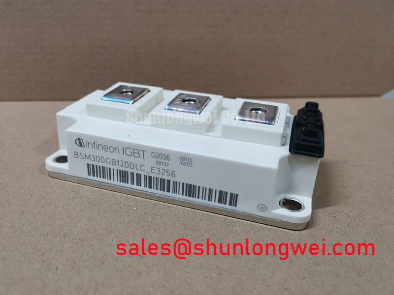
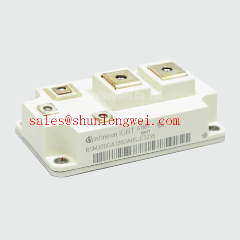
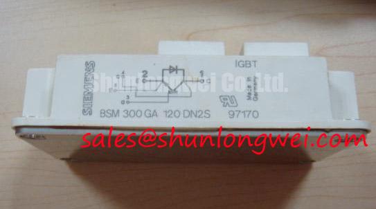
Begin incoming inspection by confirming the BSM300GA12DN2S marking, checking the module housing and terminals for visible damage, and comparing the nameplate rating with the replacement record. The official product data supplied for this Infineon device identifies a 1200.0 V rated voltage, a 300.0 A rated current, and a module package. These values establish the component identity and electrical rating for procurement and system evaluation; they do not replace the switching, thermal, isolation, or gate-drive limits required from the applicable manufacturer documentation.
| Parameter | Official specification | Engineering use |
|---|---|---|
| Manufacturer | Infineon | Confirm the brand and full ordering code during incoming inspection |
| Product model | BSM300GA12DN2S | Use the complete code when matching service records and mechanical drawings |
| Rated voltage | 1200.0 V | Compare with the converter DC-link operating boundary and transient test results |
| Rated current | 300.0 A | Evaluate together with switching frequency, case temperature, cooling, and duty cycle |
| Package | Module | Verify terminal arrangement, mounting interface, and busbar clearance from the applicable drawing |
For an industrial inverter welder or medium-frequency induction heating power supply, the device should be evaluated as part of the complete switching leg rather than by current rating alone. The system integrator should verify the original gate-drive voltage, pulse-width range, switching frequency, fault protection, cooling path, and DC-link conditions from the equipment documentation. The listed 1200.0 V and 300.0 A values are official product parameters supplied for this product page, while application limits depend on the complete electrical and thermal design.
Transient Dynamics and Electrical Design for the BSM300GA12DN2S
During a replacement assessment, isolate the gate-drive circuit before applying a control signal. Identify the gate, emitter, collector, and auxiliary terminals from the correct Infineon documentation rather than assuming that a mechanically similar module has the same terminal order. With the module unpowered and fully discharged, use a suitable meter to compare the gate-to-emitter and collector-to-emitter readings against a known-good reference. A diode-mode reading can help identify an unexpected junction path, but it is not a substitute for a controlled semiconductor test or a switching waveform inspection.
The choice between an optocoupler gate interface and a digital coreless transformer interface is a system-level decision. Designers should verify the isolation rating, working voltage, creepage, clearance, propagation delay, common-mode transient immunity, and fault response of the selected driver. These properties are not included in the official parameter set supplied for this page, so they should not be treated as guaranteed characteristics of the BSM300GA12DN2S. A driver with insufficient transient immunity can produce an unintended gate pulse during a fast collector-emitter transition, while excessive propagation mismatch can disturb the timing of a half-bridge.
Keep the power switching loop and gate-control loop physically separate where the mechanical layout permits. The gate return should follow the intended emitter reference with a short, low-impedance path, and the driver supply should be decoupled according to the driver manufacturer’s instructions. Final clearance and creepage values must be selected from the working voltage, pollution environment, insulation system, and applicable safety standard. Do not infer reinforced isolation performance or a specific kilovolt test value from the IGBT module’s 1200.0 V rating.
When a repaired inverter welder shows intermittent triggering, compare the gate-emitter waveform at the module terminals rather than at the driver output alone. Check the off-state level, pulse timing, ringing, and the relationship between the gate waveform and collector-emitter transition. If the signal differs from the known-good phase, inspect the gate-return path, connector contact pressure, driver isolation barrier, and local decoupling before replacing the power module again. The official Infineon IGBT Modules and Discretes portfolio provides useful manufacturer-level context for confirming the relevant device family and application documentation.
💡 Bench Tip: Keep the module protected against ESD and record cold-state meter readings from a known-good reference before applying any gate-drive or DC-link voltage.
Assembly Integrity and Layout Architecture
The mechanical installation must preserve a flat mounting interface, stable terminal pressure, and an electrically controlled busbar path. Confirm the original fastener type, washer arrangement, heatsink flatness, and thermal interface method from the equipment service documentation. A generic mounting practice is to tighten fasteners progressively and evenly, but the correct torque remains installation-specific unless stated by the applicable module drawing. Avoid treating a common mechanical practice as an official parameter of this Infineon model.
For current sharing in parallel paths, the positive temperature coefficient often associated with the on-state voltage of IGBT structures can support a stabilizing tendency under suitable conditions. That observation is a Design Consideration, not a guarantee that parallel operation will be balanced. The system designer should match conductor resistance, busbar geometry, gate-drive timing, thermal coupling, and current-sensing locations. Dynamic current imbalance can still arise from unequal stray inductance or gate-loop impedance even when static measurements appear similar.
Route symmetrical gate wiring for phases that must switch with comparable timing. Avoid placing a high-current commutation conductor directly beside a sensitive gate-return path when the arrangement increases magnetic coupling. Minimize parasitic loop inductance to reduce turn-off overshoot, then verify the actual collector-emitter peak with a properly rated differential probe during switching tests. The required inductance target, snubber value, and switching speed are system-determined and should be calculated from the DC-link condition, load current, gate resistance, and measured waveform.
A film snubber may be considered when the measured commutation waveform shows excessive ringing or when the equipment design requires additional local transient control. Its placement should be close to the relevant power loop, with short, wide connections and a voltage rating suitable for the measured transient environment. Designers should confirm capacitor heating, pulse-current capability, and interaction with the main DC-link network rather than selecting a value from a generic replacement rule.
In a welding inverter, inspect the busbar after a fault event for discoloration, loosened joints, punctured insulation, and evidence of uneven contact. In an induction heating supply, also review the relationship between the switching bridge, resonant network, and current sensor. The BSM75GB120DN2 may be reviewed as a reference for a related power stage, but electrical compatibility must be established from the original topology, terminal definition, and ratings rather than from package appearance.
Preventing Spurious Faults with Symmetrical Busbar Geometry
During bench diagnosis, connect the oscilloscope reference and probe loop according to the probe manufacturer’s safety instructions. A long measurement ground lead can create ringing that is not present in the power circuit, so compare the result with a suitable differential measurement method. Record the DC-link voltage, collector-emitter waveform, gate-emitter waveform, load current, and switching temperature together. This allows the engineer to distinguish a device problem from measurement-loop resonance, busbar inductance, driver timing, or load-network behavior.
The transient relationship can be considered in the form that the observed peak voltage rises with both stray inductance and current-change rate. This is an Engineering Calculation principle, not a rated characteristic of the BSM300GA12DN2S. Designers should reduce the high-current loop area, keep the commutation path compact, and validate peak voltage against the module’s applicable switching limits and the system DC-link voltage. A fixed inductance threshold should not be assigned without the original mechanical drawing, operating current, switching profile, and measurement method.
Planar busbar construction can help maintain a predictable current path, but its suitability depends on insulation coordination, mechanical spacing, fault energy, and the enclosure. Check that the positive and negative conductors maintain the intended overlap and that fast-switching paths do not include unnecessary joints or narrow necks. If a snubber is fitted, position it where it can control the actual commutation loop rather than at a visually convenient but electrically remote location.
When a protection circuit trips during no-load testing, do not assume that the IGBT is defective. Compare the gate pulse timing, desaturation or overcurrent feedback, DC-link ripple, current-sensor polarity, and auxiliary supply stability. A mismatch may indicate an impedance or timing problem; verify it against the known-good signal path with controlled energy and appropriate isolation. The service team should also inspect connectors and crimped terminals because intermittent contact can create switching behavior that resembles a semiconductor fault.
The related BSM75GD120DLC can be reviewed as a neutral option during a maintenance material comparison, subject to complete verification of voltage, current, pin assignment, package dimensions, gate characteristics, thermal behavior, and protection requirements. It should not be treated as a universal substitute for the BSM300GA12DN2S without a documented compatibility review.
Benchtop Waveform Tuning and High dv/dt Cross-Conduction Control
Use a current-limited, isolated test arrangement when bringing a repaired power stage back to operation. Begin with gate-drive verification at low system energy, then confirm that complementary switches have the intended dead time and that neither gate waveform is being disturbed by the opposite device’s collector-emitter transition. The exact timing must be established by the system designer from the driver, load, switching speed, and protection response; it is not specified by the basic 1200.0 V and 300.0 A product data alone.
An active Miller clamp can be considered where high dv/dt coupling threatens to raise the off-state gate voltage. The selected driver should be checked for clamp activation timing, sink-current capability, isolation behavior, and compatibility with the module’s gate network. Negative gate bias is also a possible design approach in some switching systems, but the permitted value must come from the applicable Infineon gate-drive data and the driver design. Do not apply a negative voltage range as a default setting for this module without confirming the manufacturer’s limits.
Cross-conduction troubleshooting should begin with simultaneous measurement of both gate-emitter signals and the phase-leg current. Look for overlap, delayed turn-off, excessive gate ringing, driver supply bounce, and a false fault signal. If the waveform changes when the probe is moved, reassess the measurement setup before modifying the gate resistor. Any damping adjustment is a Typical Starting Point for controlled bench tuning only; the final setting must be validated for switching loss, junction temperature, electromagnetic behavior, and fault response.
For a field replacement in an industrial inverter welder or medium-frequency induction heating supply, verify the complete service chain: module rating, terminal mapping, cooling interface, gate-driver isolation, protection timing, busbar geometry, and waveform margins. The technical article Wide Bandgap Revolution can provide broader engineering context when the repair team is comparing switching technologies, but it does not replace the Infineon documentation required for this specific silicon IGBT module.
Procurement teams should retain the full model code, rated voltage, rated current, package information, equipment position, and incoming inspection record. System engineers should complete the electrical and thermal validation before returning the repaired converter to service.