

Content last revised on October 11, 2026
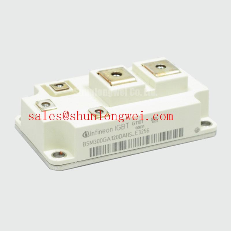
BSM300GA12DA11S Circuit Protection & Reliability: Calibrating Planar Symmetrical Busbar Geometry
Turn off overshoot is strongly influenced by the commutation loop formed by the module terminals, DC link capacitor, busbar, and freewheel path. A practical design consideration is to keep the outgoing and return current paths physically close and electrically symmetrical, reducing stray inductance and limiting the voltage generated during rapid current change. The relationship between peak switching voltage, DC link voltage, loop inductance, and current slew rate should be assessed as one system rather than inferred from the module voltage rating alone.
Use a properly rated differential voltage probe at the module power terminals and measure the waveform with the same probe placement used during commissioning. Probe ground leads can introduce misleading ringing, so the measurement connection should have a short, controlled loop. If the transient approaches the system protection threshold, review the physical position of the snubber, DC link film capacitor, and commutation return path before changing gate resistance.
Snubber selection is a system engineering task. The capacitor, resistor, pulse energy capability, and parasitic inductance must be evaluated against the actual switching waveform. A symmetrical planar busbar can improve current sharing between parallel paths, while adequate clearance around high potential conductors supports safer probing and insulation coordination. The required spacing remains dependent on working voltage, pollution level, altitude, insulation system, and applicable equipment standard.
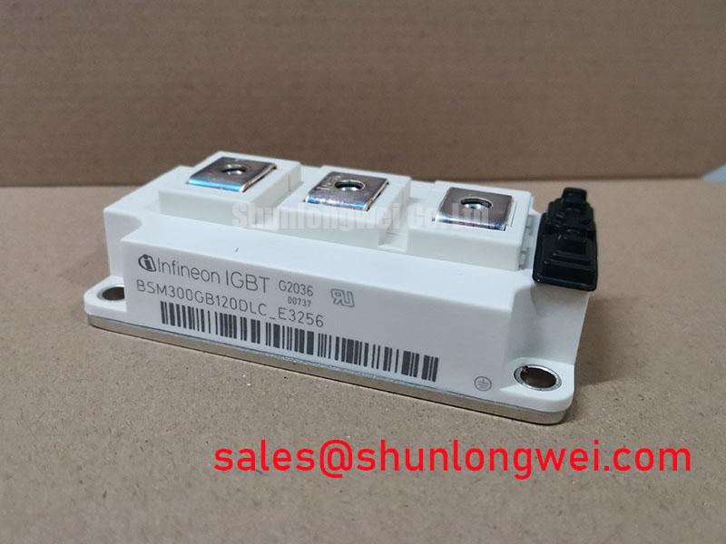
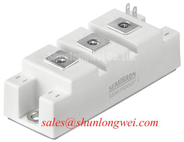
For a neutral replacement assessment, engineers may place the FD300R12KE3 beside the BSM300GA12DA11S in the sourcing review, but internal circuit configuration, gate behavior, diode recovery, terminal geometry, and thermal limits must be checked against the original circuit. This comparison does not establish interchangeability. The following table records the BSM300GA12DA11S ratings without assigning unverified ratings to the comparison device.
| Evaluation item | BSM300GA12DA11S | Replacement review requirement |
|---|---|---|
| Manufacturer | Infineon | Confirm manufacturer documentation |
| Voltage rating | 1200.0 V | Match or exceed the equipment requirement |
| Current rating | 300.0 A | Assess rating conditions, pulse current, and thermal operating point |
| Package classification | Module | Match mounting and terminal interfaces |
Field Diagnostics & Commissioning: Dynamic Power Loss Dissipation and Multi R Thermal Models
During pulsed overload commissioning, evaluate the complete thermal path from semiconductor junction to case, interface material, heatsink, and cooling medium. A transient thermal model normally uses several resistance and capacitance elements to represent short pulse heating and the slower response of the case and heatsink. The engineer should calculate junction temperature from the measured or validated case temperature, power waveform, pulse duration, and the applicable thermal impedance data for the exact module.
Do not treat the 300.0 A rating as a universal operating current. Actual dissipation depends on collector current, gate drive, switching conditions, junction temperature, duty cycle, and cooling performance. For an induction heating supply, record the pulse envelope rather than relying only on an average current meter. A current probe and synchronized voltage measurement can help separate conduction loss from switching loss when the waveform contains short, high power intervals.
Protection coordination also deserves a dedicated review. A high speed semiconductor fuse should be evaluated through its clearing behavior, prospective fault current, let through energy, and coordination with the module’s documented fault withstand limits. Fuse I²t is only useful when applied with the correct pre arcing and clearing data for the actual fuse and circuit. A fuse alone should not be assumed to protect the IGBT against a short circuit; fast electronic fault detection and controlled shutdown must be coordinated with the module’s documented limits. The gate driver should be disabled through an independent fault path when practical, while the DC link discharge method should be verified during service procedures.
For rectifier and inverter assemblies, the upstream device should be considered as part of the same energy path. The FZ1200R12KF4 may appear in a related power conversion stage review, but its electrical role and switching behavior must be assessed separately from the BSM300GA12DA11S. Infineon’s IGBT portfolio provides broader device family context for this type of evaluation.
Transient Dynamics & Electrical Design: High dv/dt Cross Conduction Shoot Through
High dv/dt can couple through the Miller capacitance and gate return path, producing an unintended gate voltage excursion on the inactive switch. The first design action is to separate power current from gate control current and return the driver reference through a low impedance path. Gate loop area should be minimized, and the driver should be located close enough to the module interface that parasitic coupling remains controllable.
An active Miller clamp can provide a low impedance discharge route during the opposing switch transition. Whether it is required depends on the driver architecture, switching speed, common emitter arrangement, and measured gate waveform. Negative gate bias is a possible design option in suitable driver systems, but its polarity, magnitude, transient behavior, and insulation coordination must be validated against the module and driver documentation rather than selected as a universal setting.
Check the gate to emitter waveform with an isolated differential probe during double pulse or controlled low energy commissioning. Look for a transient plateau, delayed turn on, asymmetric rise and fall behavior, or a difference between the command signal and the module pin voltage. These observations can indicate coupling, driver saturation, poor reference routing, or an unsuitable gate network; they do not establish a single failure cause without waveform correlation.
Freewheel diode reverse recovery also influences EMI and overshoot. A softer recovery characteristic can reduce abrupt current transfer, while a fast but heavily oscillatory recovery event may increase radiated and conducted noise in the surrounding loop. The appropriate tradeoff depends on switching frequency, busbar structure, snubber placement, and filter design. The module itself cannot be described as independently certified for complete equipment EMC compliance. Engineers should consult Infineon Technologies documentation and validate the finished equipment under its applicable EMC requirements.
💡 Pro Tip: Keep the gate driver return and power commutation return physically distinct, then confirm the resulting gate margin and collector emitter transient with controlled oscilloscope testing before applying full production load.
BSM300GA12DA11S Thermal Electrical Optimization: Main Terminal Pinout Mechanical Alignment Practical Tuning
Mechanical alignment at the main terminals affects electrical reliability because a misaligned busbar can transfer bending force into the module terminal structure. Before tightening, place the busbar naturally over the terminal pattern and check that the conductor does not need to be levered into position. The fastener, washer arrangement, thread engagement, and tightening sequence should follow the module’s mechanical documentation and the equipment assembly standard.
Thermal interface material should form a continuous, controlled interface between the module base and heatsink. Excess compound can contaminate nearby surfaces, while insufficient coverage can leave localized air gaps. The heatsink should be clean, flat within its specified assembly tolerance, and supported so that tightening does not twist the module. Any required torque must come from the applicable mechanical specification rather than a generic value applied to every module family.
During service inspection, compare terminal alignment, washer seating, heatsink contact marks, and signs of movement after thermal cycling. Vibration can gradually change contact pressure even when the electrical circuit initially passes a static test. For high voltage assemblies, also review creepage and clearance around the main terminals, contamination paths, and the effect of enclosure altitude on insulation performance. Cosmic ray induced single event burnout and high altitude behavior require application specific reliability analysis; no universal FIT value or lifetime figure should be assigned to this part without an authoritative source and defined operating profile.
The 1200 V CoolSiC™ MOSFET technology discussion can provide useful system level context when engineers compare switching technologies in three phase conversion, but it does not replace the electrical and mechanical qualification of the BSM300GA12DA11S in its intended topology.