Content last revised on September 26, 2026
Field Diagnostics & Commissioning: Auxiliary Emitter Return Trace Separation in MG50M2CK2 Topologies
During commissioning, first isolate the DC link and discharge the system according to the equipment service procedure. Check the module body, mounting surface, power terminals, and gate connections for contamination, mechanical damage, or signs of overheating. A resistance comparison between corresponding power terminals can help identify an abnormal short condition, but the measured value must be interpreted with the connected circuit removed because bus capacitors, snubbers, and gate-drive components can affect the result.
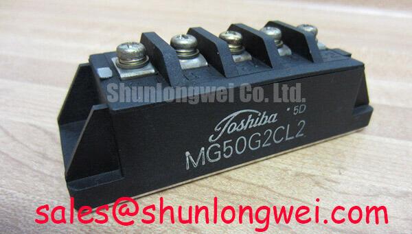
The Toshiba MG50M2CK2 is a 1200.0 V, 50.0 A IGBT module, but those ratings do not define the allowable switching overshoot in a particular inverter. The current rating must be interpreted under the conditions specified in the manufacturer’s documentation. When the original circuit uses separate power and auxiliary emitter returns, keep the high-current emitter path physically distinct from the gate-drive return path. The purpose is to prevent the voltage developed by common emitter inductance from being added to the gate-control signal. Use short, closely coupled gate-loop conductors and avoid routing the gate return alongside high di/dt collector or DC-link paths.
This is a Design Consideration rather than an additional Toshiba specification. The system designer should establish the required clearance between power conductors, control wiring, heatsink hardware, and grounded structures according to the working voltage, pollution environment, insulation system, and applicable safety standard. During troubleshooting, compare gate-to-emitter and collector-to-emitter waveforms at the module terminals with a suitable isolated measurement method. Ringing, an unexpected gate pulse, or a large difference between switching positions may indicate return-path coupling, probe-loop error, unequal wiring, or driver timing mismatch. Verify the complete signal path before changing gate resistance.
For equipment using commercial string inverter or micro-grid energy-storage power stages, the module should be evaluated against the actual DC-link voltage, switching frequency, current waveform, fault-clearing time, and cooling arrangement. The related MG100Q1ZS40 may be reviewed as a separate Toshiba reference device, but electrical and mechanical interchangeability must be established by the system engineer rather than assumed from a similar product category.
MG50M2CK2 Thermal-Electrical Optimization: Isolated DC-DC Power Supply Sizing for Practical Tuning
The isolated gate-drive supply must be assessed as part of the complete switching system. Designers should verify the required output voltage, isolation barrier, startup behavior, fault response, common-mode transient performance, and grounding arrangement from the driver and converter documentation. Reinforced isolation and common-mode transient immunity are requirements to evaluate for the gate-drive isolation system, not characteristics that can be inferred from the MG50M2CK2’s voltage rating.
For practical tuning, inspect the gate supply at the module pins rather than only at the isolated converter output. Undershoot during turn-on, supply movement during repetitive switching, or a floating reference can create apparent gate-drive faults. Minimize parasitic loop area, separate control returns from high-current paths, and validate the result with differential probing under the highest expected switching stress. The Precision Gate Drive Design guide can provide broader engineering context, while the final gate network remains system-determined.
Thermal installation begins with a clean, flat heatsink interface and an even thermal interface layer selected for the module and heatsink surfaces. A uniform, thin application is generally preferred to reduce thermal resistance and mechanical tilt, but the material thickness and mounting torque must follow the module documentation and the TIM supplier’s instructions. Use a staged cross-pattern tightening sequence so the base does not cant against the heatsink. Do not infer an approved screw torque, isolation voltage, or transient thermal impedance from the product name alone.
Maintenance Note: During scheduled service, monitor contact temperature trends, inspect the thermal interface for drying or pump-out, and verify that the heatsink airflow path remains clear.
MG50M2CK2 Circuit Protection & Reliability: Calibrating Symmetrical Busbar Geometry for High Current
Busbar geometry should be checked before the first loaded run. Keep parallel current paths similar in length and shape, position the DC-link decoupling close to the switching loop, and avoid a layout in which one device position receives a materially different stray inductance. The objective is to reduce unequal voltage overshoot and dynamic current imbalance; the acceptable result must be confirmed through oscilloscope measurements and thermal observations on the actual assembly.
In parallel IGBT arrangements, a positive temperature coefficient of collector-emitter saturation voltage, where supported by the device characteristics at the operating current, can support steady-state current sharing, but it does not by itself guarantee equal dynamic current during turn-on or turn-off. Match gate-loop routing, driver timing, emitter-return geometry, and power-path impedance. If one position shows higher temperature or a different switching waveform, inspect mechanical contact, gate resistance, wiring symmetry, current-sensor placement, and busbar coupling before attributing the behavior to the module.
Fast semiconductor fuses should be coordinated with the converter’s fault strategy using the fuse manufacturer’s I²t information, the module’s short-circuit withstand data if available, DC-link energy, and the protection detection delay. No fuse rating or short-circuit duration is provided here, so the selection must be calculated and verified by the equipment designer. Do not assume that a fuse alone will protect the IGBT against a short circuit. A test plan should include gate inhibition, fault-current measurement, DC-link discharge behavior, and post-test inspection of the module and fuse. The same approach applies to pre-charge faults and hard short circuits.
High-voltage spacing is also a system issue. Confirm creepage and clearance around the module terminals, busbars, fasteners, insulating barriers, and contaminated surfaces using the applicable insulation standard and environmental assumptions. The 1200.0 V rating identifies the device class; it does not specify the finished equipment’s required spacing or safety certification.
Benchtop Waveform Tuning: Mitigating Stress via Junction-to-Case Thermal Network Simulation on MG50M2CK2
Bench testing should begin with a controlled switching condition and a documented thermal boundary. Record the case temperature near the module mounting area, the DC-link voltage, current waveform, pulse duration, repetition rate, and switching-node overshoot. The MG50M2CK2’s 1200.0 V voltage rating and 50.0 A current rating must be interpreted using the applicable manufacturer data, including rating conditions, junction-to-case thermal values, and transient thermal curves.
A multi-RC thermal model can be used as an Engineering Calculation when its resistance and capacitance values come from the correct Toshiba thermal network or are fitted to the applicable manufacturer thermal data. The model should combine conduction loss, switching loss, pulse duration, duty cycle, case temperature, and the actual heatsink response. Peak junction temperature should then be compared with the manufacturer’s permitted operating conditions. Do not substitute a generic IGBT thermal curve, because package construction, chip arrangement, interface conditions, and measurement reference can change the result.
Waveform tuning should address both electrical and thermal stress. Minimize stray inductance to control turn-off overshoot, then verify the measured peak collector-to-emitter voltage against the device’s applicable voltage limit, with appropriate design margin and the final busbar and probe arrangement. Adjustments to gate damping are Typical Starting Points for bench tuning only; every change should be checked for switching loss, gate stability, conducted noise, and device temperature. The interleaved boost topology described in Interleaved Boost Converter for Reduced DC-Link Input Ripple Current may be relevant when evaluating ripple-current behavior, but topology-level benefits depend on control timing, layout, and load conditions.
After thermal cycling or extended bench operation, repeat the visual inspection, terminal checks, gate-signal comparison, and heatsink temperature survey. Any abnormal result should be compared with a known-good waveform and the original equipment documentation before a replacement decision is made.