

Content last revised on September 24, 2026
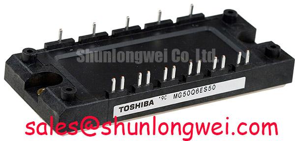
MG50Q6ES50 Operational Boundaries: Evaluating Gate Drive Loop Geometry Before Limits
During installation, trace the complete gate-drive loop from the driver output to the module gate terminal and back through the intended emitter return. The objective is to keep the control-current path distinct from the high-current commutation path. Shared copper can introduce emitter mutual coupling, causing the driver to sense a voltage that includes power-loop noise rather than the actual gate-emitter condition. This can appear during commissioning as ringing, irregular switching delay, or an unexpected difference between the upper and lower switching devices.
Design Consideration: Keep the gate-drive conductors short and closely coupled, route the return beside the outgoing gate path, and avoid placing the control return inside the high di/dt collector-emitter current loop. Where the module and driver arrangement provides a separate auxiliary emitter connection, the control return should be routed independently from the main power emitter conductor. The final spacing and copper geometry remain system-dependent and should be validated with differential probing during switching tests.
Do not assume that a visually short connection has low electrical impedance at the switching edge. Connector pins, vias, copper neck-downs, and long measurement leads can all contribute to the observed waveform. A practical commissioning check is to compare the gate-emitter waveform at the module terminals with the signal measured at the driver output. If the two waveforms differ materially, inspect the return path and probe arrangement before changing the gate resistor or driver supply.
The 600 V rating should also be assessed against the complete DC-link and transient environment. A switching device can remain within its static voltage rating while the local turn-off overshoot approaches an unsafe condition. Designers should verify the collector-emitter peak, gate-emitter disturbance, and switching temperature under the actual load profile rather than using the catalog voltage alone as a complete approval criterion.
MG50Q6ES50 Thermal-Electrical Optimization: Controlling Parasitic Gate Disturbance
Parasitic capacitance between the power terminals and gate circuit can transfer a rapid voltage transition into the gate loop. This is often discussed as Miller-induced gate disturbance. Its severity depends on the switching waveform, gate impedance, common-emitter inductance, driver strength, and the physical arrangement of the module, busbar, and gate-drive board. The MG50Q6ES50 product information supplied for this page does not establish a universal gate voltage, negative-bias value, switching speed, or capacitor value, so those settings must come from the original design or validated bench testing.
As an Engineering Recommendation, use a driver arrangement capable of controlling the off-state gate impedance and consider an active Miller-clamp function where the system’s dv/dt and cross-conduction risk justify it. A negative gate bias may be evaluated in suitable driver architectures, but its polarity, magnitude, transient behavior, and insulation coordination must be confirmed against the module documentation and driver ratings. It should not be introduced as a default replacement setting.
Thermal and electrical optimization should be performed together. A clean gate waveform does not compensate for inadequate heat removal, while a well-sized heatsink cannot correct an uncontrolled turn-off spike. Designers should measure case temperature, switching-node voltage, gate-emitter voltage, and load current during representative operation. The result should then be compared with the approved electrical and thermal limits for the equipment, not with a generic IGBT rule of thumb.
Busbar construction deserves the same attention as the gate circuit. A compact, symmetrical commutation path helps reduce stray inductance and limits the voltage generated during rapid current change. Film capacitors used for local high-frequency support should be positioned according to the power-loop current path, with short, broad connections and minimal unnecessary via transitions. The required capacitance, voltage rating, ripple capability, and placement are determined by the DC-link topology and measured transient response.
Power conversion equipment may also contain an NTC thermistor for temperature sensing or inrush-related functions, but the presence, location, and electrical role of such a device must be confirmed from the actual circuit. The general temperature-dependent behavior of thermistors is described in this thermistor reference; it should not be treated as a product-specific specification for the MG50Q6ES50.
Transient Dynamics and Electrical Design: Desaturation Detection on MG50Q6ES50
Desaturation protection is a system-level method for detecting an abnormal rise in the IGBT’s collector-emitter voltage while the device is commanded on. Its response depends on the gate driver, blanking behavior, sensing network, isolation method, and soft turn-off strategy. The MG50Q6ES50 data provided here confirms a 600 V, 50 A Toshiba IGBT Module, but it does not establish a universal detection delay or short-circuit withstand interval. Those values must be taken from the applicable Toshiba documentation and the selected driver design.
When integrating the module into an inverter, verify that the protection circuit can distinguish a legitimate switching transition from an overcurrent or short-circuit event. The sensing path should be physically separated from noisy power nodes, and its reference should remain stable during the commutation event. Designers should test fault response at controlled DC-link voltage and load conditions, then verify that the gate driver limits the energy applied to the module without creating an excessive turn-off voltage transient.
A two-stage soft turn-off sequence may be considered when the driver supports it. The first stage reduces the gate command in a controlled manner, while the second stage completes turn-off after the fault condition is confirmed. This is an Engineering Recommendation, not an inherent feature claim for the MG50Q6ES50. The final timing and gate-current profile should be selected from the driver manufacturer’s application data and validated against measured collector-emitter voltage.
For compact industrial inverters and CNC spindle drives, fault testing should include stalled-load behavior, abnormal phase conditions, and controlled interruption of the gate command. Observe whether the fault signal is clean, whether the complementary switch remains inhibited as intended, and whether the DC-link voltage remains within the system’s transient margin. The reference material on field-stop trench IGBTs and intelligent modules provides useful industry context for protection and switching considerations, but it does not replace Toshiba’s specifications for this part.
Bench Diagnostic: Disconnect power and allow the DC link to discharge before removing gate-driver wiring or handling the module terminals.
Field Diagnostics and Commissioning: High-Frequency Commutation Loop Inductance
When a repaired inverter shows repeated overvoltage alarms, begin with measurement rather than immediate component substitution. Confirm the DC-link voltage, inspect the laminated or parallel busbar arrangement, check fastener and terminal condition, and compare the switching-node waveform with a known-good assembly where available. The voltage rise associated with stray inductance increases as current changes more rapidly, so the measured turn-off peak must be evaluated together with the actual current slope and local loop geometry.
The commutation loop should be kept compact and geometrically balanced. Positive and return conductors placed close together reduce the enclosed loop area, while asymmetry can increase magnetic coupling and produce different voltage stress on parallel paths. Any target inductance value must be calculated and verified for the specific busbar, capacitor, module, and switching condition; it should not be presented as a universal MG50Q6ES50 requirement.
Snubber selection is also system-dependent. Designers should verify capacitor pulse capability, dielectric voltage rating, repetitive current, physical lead inductance, and temperature rise. Placement is often as important as nominal capacitance because a remote capacitor may not effectively control the local switching node. Use suitable high-bandwidth voltage measurement techniques and confirm that the probe connection does not create an artificial ringing path.
For topology assessment, the operating behavior of a quasi-resonant or half-bridge arrangement can materially change the stress seen by the switching module. The article Resonant Topologies in Home Appliances can be used as a reference when comparing commutation paths and soft-switching assumptions. It does not establish compatibility or ratings for the MG50Q6ES50.
Before releasing a repaired assembly, verify the module identity, the 600 V voltage class, the 50 A current class, terminal polarity, gate-drive compatibility, cooling interface, and protection behavior. The MG100Q1ZS40 may be reviewed as a separate Toshiba module for comparative sourcing analysis, but substitution requires a complete electrical, mechanical, thermal, and control-interface check rather than a rating-only comparison.