

Content last revised on October 11, 2026
Assembly Integrity & Layout Architecture: Implementing Baseplate Thermal Grease Layer Control for MG75J2YS40
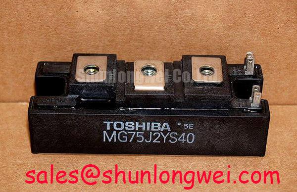
Inspect the heatsink contact surface and the previous thermal grease imprint before mounting the MG75J2YS40; uneven transfer can reveal assembly conditions worth correcting before electrical commissioning. The Toshiba IGBT module has a 600 V collector-emitter voltage rating and a 75 A collector-current rating under the specified datasheet conditions. These ratings do not establish permissible operation at every temperature or duty cycle. The module’s mechanical documentation should be consulted for mounting dimensions, terminal assignments, and tightening torque.
Design Consideration: thermal interface material should fill surface irregularities without becoming an unnecessarily thick thermal barrier. Clean the mating surfaces using a compatible process, inspect for raised burrs, and evaluate baseplate flatness against the mechanical drawing. A grease imprint can help assess coverage, but it cannot by itself establish acceptable thermal resistance. Select application thickness through the interface material instructions, mounting geometry, and thermal validation rather than applying a universal micrometre target.
Bring the mounting screws into contact progressively, using an alternating sequence to distribute pressure across the baseplate. Apply the specified final torque for the module and mounting hardware. Do not use screw force to flatten an incorrectly seated assembly. Where curvature or poor contact is suspected, inspect the supporting surface and mounting arrangement before changing grease quantity. Keep grease away from electrical contact surfaces and preserve access for terminal inspection.
Design Consideration: during a repeatable load test, compare case temperature, heatsink temperature, and their response over time. The relationship between material properties and transient heat spreading is explained by thermal diffusivity, but that general principle does not identify this module’s substrate construction. Likewise, sintering describes a materials process, including applications in electronic packaging; it is not evidence that MG75J2YS40 uses silver-sintered die attachment.
Field Diagnostics & Commissioning: SCSOA Overcurrent Protection: Implementing in MG75J2YS40 Topologies
Trace the fault-detection signal from the sensing circuit to the gate-driver shutdown output before energizing the power stage. Design Consideration: short-circuit protection must account for detection delay, signal filtering, driver response, and the current decay during shutdown. Establish the permitted sequence from the applicable short-circuit safe operating area conditions, rather than treating a generic microsecond deadline as an MG75J2YS40 rating.
A type-I fault involves switching into an existing short circuit; a type-II fault develops while the device is already conducting. Their current and collector-voltage trajectories differ, so protection evaluation should address the relevant fault conditions separately. Desaturation sensing or another current-monitoring method needs coordinated thresholds and blanking behavior. Two-stage soft turn-off can help manage inductive voltage overshoot, but its timing and gate discharge profile remain system-dependent engineering choices.
For sourcing comparisons, retain the MG75J2YS40 electrical boundary as the reference and examine the MG400V2YS60A as a separate Toshiba candidate, not a presumed interchangeable upgrade. The comparison below distinguishes established product data from the documentation needed for replacement assessment.
| Comparison item | MG75J2YS40 | MG400V2YS60A |
|---|---|---|
| Manufacturer | Toshiba | Toshiba |
| Collector-emitter voltage rating | 600 V — consult datasheet for applicable limits | Consult Datasheet |
| Collector-current rating | 75 A — under specified datasheet conditions | Consult Datasheet |
| Package and mounting details | Consult mechanical drawing | Consult Datasheet |
| Replacement assessment | Reference device | Compare circuit, terminals, mounting, switching behavior, and protection requirements |
When evaluating an electric material-handling or low-voltage forklift traction controller, designers should check whether its power-stage topology, cooling arrangement, and driver protection support this device. Inspect the upstream rectifier, precharge path, and DC-link circuit as separate subsystems. The MG30G2CL3 can be considered in a complementary-stage component review only after its actual circuit function and ratings are matched; the association does not establish it as a rectifier or a direct substitute.
Preventing Spurious Faults: High dv/dt Cross-Conduction Shoot-Through Guidelines for MG75J2YS40
Capture the inactive switch’s gate-to-emitter waveform during opposite-arm switching when unexplained current spikes or protection trips occur. Design Consideration: collector-voltage transitions can couple displacement current through gate-collector capacitance, disturbing the off-state gate voltage. Distinguish that behavior from commanded overlap, diode recovery, and measurement pickup before changing the driver.
A low-impedance off-state path can reduce unwanted gate movement. An active Miller clamp is one possible driver feature, provided its activation behavior, current capability, and connection geometry suit the circuit. Negative gate bias is another system-level option, but its magnitude must remain within the device’s gate-voltage limits and the driver’s operating requirements. Neither approach justifies assigning an unsupported bias voltage to MG75J2YS40.
Measure close to the module’s gate and emitter connections with a suitably rated differential probe and a controlled measurement loop. Compare driver-output behavior with the waveform at the device terminals. A disturbance appearing only at the module can point toward connection impedance or coupling; a disturbance already present at the driver requires investigation of the driver supply, reference path, and control signals.
Design Consideration: freewheeling-diode reverse recovery can contribute current transients and excite parasitic inductance. Recovery softness describes waveform behavior, but no numerical softness factor is established here for MG75J2YS40. Evaluate current recovery and voltage ringing together before attributing emissions or nuisance trips to one mechanism. Long motor cables introduce a separate reflected-wave problem at the motor terminals; assess cable characteristics, termination, and any output-filter requirement independently of the module’s collector-voltage waveform.
Preventing Spurious Faults: Optimizing Gate Drive Loop Geometry for MG75J2YS40
Route the gate-drive outgoing and return conductors together, keeping their loop separate from the main commutation-current path. Design Consideration: shared emitter-path inductance can shift the driver’s reference during current transitions, altering the effective gate-to-emitter voltage. Where the terminal arrangement supports a separate auxiliary emitter connection, use the documented connection; do not assume the package contains a dedicated Kelvin emitter terminal.
Position the driver return at the appropriate device reference connection rather than allowing it to share a long, high-current conductor. Keep adjacent switching-node copper from unnecessarily coupling into gate traces, and establish clearances from the equipment’s working voltage, insulation requirements, and applicable standards. Check connector routing and service wiring as part of the loop: a compact circuit board does not compensate for a long external gate harness.
Pro Tip: consider closely coupled, balanced DC-link busbar paths to reduce commutation-loop inductance, then verify collector-voltage overshoot and gate behavior with a controlled double-pulse test.
During that test, evaluate turn-off overshoot at the device terminals alongside DC-link voltage and current decay. Change one layout or drive variable at a time so the measurement identifies its effect. Oscillation can involve gate-loop impedance, common-emitter coupling, power-loop resonance, or probing artifacts; waveform comparison is more useful than assigning a single cause from appearance alone.
For repeated operating validation, record the mounting condition, cooling state, driver configuration, and test waveform settings so later measurements remain comparable. The Power Electronics Masterclass provides broader selection and reliability context, while MG75J2YS40 acceptance should remain tied to the equipment’s documented electrical and thermal checks. After a routing change, recheck both normal switching and protection shutdown to ensure reduced ringing has not compromised fault response.