

Content last revised on October 12, 2026
Field Diagnostics & Commissioning: Dynamic Power-Loss Assessment and Multi-RC Thermal Modeling in BSM100GB170DN2 Topologies
- Check cold terminal impedance with the DC link fully isolated and discharged.
- Inspect baseplate contact, thermal interface coverage, busbar alignment, and mounting hardware.
- Confirm gate-driver isolation and wiring condition before applying any switching command.
- Record the installed module rating against the original traction inverter documentation.
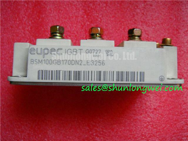
BSM100GB170DN2 is an Infineon IGBT module with an official rated voltage of 1700 V, an official rated current of 100 A, and a Module package designation. These are product-level specifications; allowable switching frequency, overload duration, junction temperature, and cooling performance remain system-dependent. The module is therefore evaluated by checking the power stage, gate-drive behavior, mechanical interface, and insulation condition as one working assembly.
Dynamic thermal assessment should begin with the actual switching waveform and load profile rather than the nameplate current alone. In a traction inverter, pulsed current, regenerative braking, and repeated acceleration create a transient junction temperature response that is different from steady-state operation. The thermal path should be reviewed from the semiconductor junction through the case, thermal interface, heatsink, and cooling circuit.
For a double-pulse or controlled commissioning test, capture collector-emitter voltage and current with suitably rated differential and current probes. Observe turn-on loss, turn-off overshoot, diode recovery behavior, and the duration of each load pulse. A multi-RC thermal model can then represent the junction-to-case transient response, but its resistance and time-constant values must come from the applicable manufacturer thermal data and the measured assembly. The resulting peak junction estimate should be compared with the permitted operating boundary under the tested duty cycle.
In a bidirectional DC-DC battery charger or traction auxiliary converter, thermal cycling can be influenced by both charging and discharging direction. Designers should assess the hottest switching position, the braking resistor duty, and the cooling response after repeated pulses. Keep the commutation loop physically compact and confirm the DC-link recovery behavior on the oscilloscope before increasing power.
BSM100GB170DN2 Thermal-Electrical Optimization: Baseplate Convexity Compensation and Screw Practical Tuning
Thermal contact quality depends on the complete mounting stack, not only on the heatsink rating. Clean both mating surfaces, apply a continuous and controlled thermal interface layer, and inspect for air pockets after assembly. A typical thermal interface thickness target of 50–100 µm may be used as a design consideration when compatible with the selected material and surface flatness; the system builder should follow the TIM supplier’s process limits.
Baseplate curvature or uneven heatsink flatness can concentrate pressure in a small area and leave other regions poorly coupled. Use a calibrated flatness inspection method appropriate to the assembly, then tighten the screws progressively in a diagonal sequence. The correct torque is determined by the fastener, washer, heatsink, and module mechanical documentation rather than by a generic value.
Parallel module operation requires symmetrical busbar geometry, equivalent thermal paths, and matched gate-drive routing. The positive temperature coefficient associated with collector-emitter saturation behavior can assist static current sharing, but dynamic sharing still depends on stray inductance, gate-loop impedance, timing, and layout symmetry. When a higher-current comparison is required, engineers can review the related BSM150GB170DN2 without treating it as an automatic replacement.
⚠️ Field Alert: Never adjust mounting torque while the power assembly is energized, and do not insert or remove gate-drive connections until the equipment has been isolated and discharged.
Field Diagnostics & Commissioning: Pollution Degree 3 Creepage Distances in BSM100GB170DN2 Topologies
In dusty industrial cabinets, insulation inspection must cover the module terminals, baseplate, busbar supports, and surrounding contamination paths. An insulation tester can be used to audit terminal-to-baseplate isolation at the specified test condition of at least 500 MΩ at 2.5 kV DC, provided the module documentation and the complete system safety procedure permit that test. Disconnect sensitive gate-driver electronics before applying the test voltage.
Record the result, test duration, ambient condition, and physical cleanliness. A declining reading, unstable value, or visible tracking path should trigger a controlled inspection of the DCB assembly, mounting surface, insulators, and cable routing. Do not interpret one resistance measurement as proof of switching health; insulation integrity and semiconductor conduction behavior require separate checks.
Pollution Degree 3 installation practice also requires adequate creepage and clearance for the working voltage, contamination level, material group, and applicable equipment standard. Designers should prevent dust accumulation around high-potential terminals and should verify the finished enclosure rather than relying only on the module outline. Infineon’s PrimePACK™ module information provides useful manufacturer context for module integration, while the final spacing decision belongs to the equipment design.
BSM100GB170DN2 Thermal-Electrical Optimization: Damping Tail-Current Oscillations During Practical Tuning
Tail-current oscillation should be examined at the commutation loop, where IGBT tail current, diode reverse recovery, busbar inductance, gate resistance, and driver timing can interact. Capture the relevant IGBT and antiparallel diode currents and identify the reverse-recovery peak and its rate of change during the switching event. A sharp current transition can increase voltage ringing and conducted or radiated disturbance, but the corrective setting must be derived from the measured waveform and device operating point.
As an engineering recommendation, begin bench tuning with controlled changes to turn-on gate resistance while monitoring collector-emitter overshoot, switching loss, driver waveform, and thermal rise. An RC snubber may be evaluated when ringing remains after the power loop and gate loop have been physically optimized. Its capacitance, resistance, pulse rating, and placement are system-design variables; verify the resulting dissipation and voltage margin during representative regenerative braking and battery charge-discharge cycles.
Gate-driver isolation must tolerate the measured common-mode transient behavior of the inverter. Check the isolator supply integrity, return-current path, gate-emitter voltage at the module pins, and synchronization between parallel channels. The Infineon IGBT Modules and Discretes portfolio offers broader manufacturer reference context, while the related 1200 V CoolSiC™ MOSFET Advantage in Three article can support technology-level comparison when reviewing future converter architectures.