
Content last revised on September 10, 2026
Key Ratings and Incoming Inspection: 2MBI100U4H-170
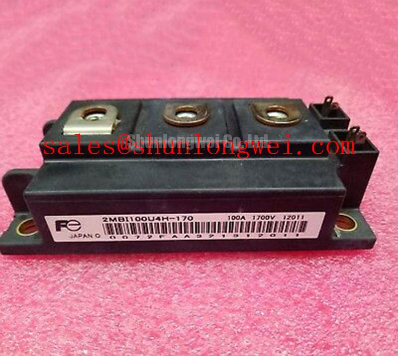
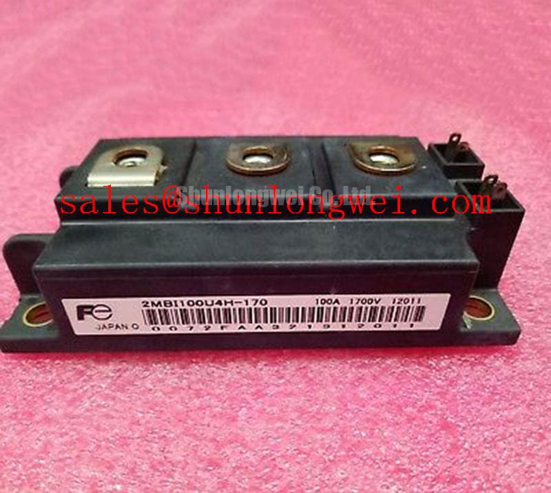
Before installation, isolate the module and perform a cold-state incoming check: confirm the marked terminal polarity, inspect the case and baseplate for mechanical damage, and verify the nameplate rating against the traction inverter service record. For the Fuji Electric 2MBI100U4H-170, the principal official ratings are a 1700 V collector-emitter voltage, 100 A continuous collector current at TC = 80°C, and 200 A pulsed collector current under the specified datasheet conditions. These values are Official Datasheet Specifications and should be checked against the actual switching frequency, cooling arrangement, and load profile before field replacement.
| Parameter | Specification | Classification |
|---|---|---|
| Collector-emitter voltage, VCES | 1700 V | Official Datasheet Specification |
| Continuous collector current, IC at TC = 80°C | 100 A | Official Datasheet Specification |
| Pulsed collector current, ICP | 200 A under the specified datasheet conditions | Official Datasheet Specification |
| Isolation voltage, Viso, AC for 1 minute | 4000 V | Official Datasheet Specification |
| IGBT thermal resistance, Rth(j-c) | 0.20 K/W | Official Datasheet Specification |
| Maximum junction temperature, Tj max | 150°C | Official Datasheet Specification |
| Baseplate mounting torque | 2.5 to 3.5 N·m | Design Consideration for M5 screws |
Assembly Integrity & Layout Architecture: Implementing Symmetrical Busbar Geometry for 2MBI100U4H-170
Use the module’s physical terminal arrangement as the reference for the first layout inspection. The positive and negative power paths should present comparable current paths to the switching devices, with busbars kept compact and arranged to reduce unequal stray inductance. This is a Design Consideration rather than a Fuji Electric guarantee for a particular cabinet layout. The final arrangement depends on the DC-link structure, switching sequence, cooling hardware, and enclosure clearances.
At the incoming inspection bench, compare the replacement module with the removed unit using terminal markings, mounting-hole position, baseplate condition, and the original wiring record. Do not infer an unmarked auxiliary terminal function from its physical location. Confirm the gate, emitter, collector, and any auxiliary connection against the applicable Fuji Electric documentation and the inverter schematic. The 4000 V AC isolation rating for one minute is an Official Datasheet Specification for the module isolation system; the assembled inverter must still be tested as a complete insulated structure because busbar spacing, contamination, cable routing, and mounting hardware affect system insulation.
The positive temperature coefficient commonly associated with IGBT on-state voltage can support steadier static current sharing when paralleled devices operate under properly matched conditions. It does not remove the need to match gate-drive timing, emitter return impedance, thermal contact, and busbar geometry. Designers should verify current balance during controlled load testing rather than assuming that nominally identical modules will share dynamic current equally.
For applications such as high-speed rail traction inverters or heavy freight locomotive propulsion converters, compatibility must be established from the original equipment documentation. Check the DC-link voltage, gate-driver interface, protection timing, cooling plate, isolation coordination, and mechanical envelope before authorizing a replacement. A higher or lower current-rated module is not automatically interchangeable. Engineers performing a neutral cross-reference may also evaluate the related 2MBI400U4H-170, but its electrical and mechanical requirements must be compared independently.
Preventing Spurious Faults: Differential Gate-Emitter Loop Routing Guidelines for 2MBI100U4H-170
Route the gate-drive signal and its emitter return as a closely coupled differential loop, keeping the control return separate from the main high-current emitter path wherever the module terminal documentation provides an auxiliary emitter connection. The purpose is to reduce common emitter coupling and prevent power-current voltage drop from appearing as an unintended gate signal. This is an Engineering Recommendation; the correct routing remains system-determined and should be confirmed with oscilloscope measurements at the module terminals.
During commissioning, monitor the gate-to-emitter waveform directly at the module rather than at the distant driver board. Look for ringing, excessive common-mode movement, unequal turn-on or turn-off timing, and changes that occur only when collector current rises. A fault indication can have several causes, including driver supply instability, grounding impedance, probe-loop pickup, protection interlock timing, or an actual switching abnormality. Compare the suspect phase with a known-good phase under the same operating conditions.
If the commutation path includes a freewheeling diode, its reverse-recovery behavior can contribute to collector-emitter overshoot and radiated noise. Verify the diode characteristics in the relevant module documentation and observe the current commutation loop with a suitable high-bandwidth probe. An RC or RCD snubber, damping network, or revised busbar path may be considered when measured ringing exceeds the system’s validated voltage margin. Component values should be selected from measured waveforms and loss calculations, not copied as universal settings.
Gate resistance, driver output impedance, dead time, and protection thresholds should be reviewed together. A slower edge may reduce ringing but increase switching loss, while a faster edge can increase voltage overshoot and electromagnetic interference. The decision should be made from measured switching loss, junction-temperature behavior, fault response, and conducted or radiated emissions at the equipment level. Fuji Electric’s Global Power Semiconductor Technologies resource provides manufacturer-level background for evaluating power semiconductor integration.
💡 Bench Tip: Keep the module and test leads under ESD control, discharge the DC-link capacitors fully, and establish a cold-state diode-test baseline before applying any powered gate signal.
Field Diagnostics & Commissioning: Turn-Off Inductive Overshoot Clamping in 2MBI100U4H-170 Topologies
Turn-off testing should begin at reduced system energy with the DC-link voltage, collector current, gate waveform, and collector-emitter voltage recorded at the module terminals. The engineering relationship between peak voltage, DC-link voltage, stray inductance, and current fall rate explains why a compact commutation loop is important: increasing either parasitic inductance or current slew raises the transient voltage component. This is an Engineering Calculation framework, not an additional product rating.
The measured peak must remain within the validated switching margin of the application and below the module’s 1700 V VCES Official Datasheet Specification. Designers should minimize the high-current commutation loop, maintain symmetrical planar busbar geometry where practical, and verify the peak margin during the actual switching test. Do not treat a calculated inductance target as a guaranteed property of the module; it belongs to the complete inverter assembly.
When a turn-off waveform shows overshoot or ringing, inspect the DC-link capacitor connection, laminated busbar joints, terminal clamping, snubber placement, probe technique, and gate-drive return path. A long oscilloscope ground lead can create a false ringing signature, while a loose power connection can produce a genuine transient. Repeat the measurement with a differential high-voltage probe and a current probe positioned around the intended commutation path.
Snubber selection should balance transient suppression against switching loss, capacitor stress, pulse current, and thermal dissipation. The correct capacitance and resistance are system-determined. Engineers should validate the network over the expected DC-link range, load-current range, temperature range, and switching pattern rather than relying on a single bench waveform. The same evaluation should include MOV coordination where the inverter uses a metal-oxide varistor for slower external surge energy. An MOV can complement, but does not replace, local semiconductor transient control, insulation coordination, or DC-link protection.
For a structured review of gate-drive behavior, parasitic inductance, thermal paths, and protection interactions, consult the IGBT Design & Integration technical reference. It can support the commissioning checklist without treating general topology guidance as a device-specific warranty or operating limit.
Preventing Spurious Faults: Thermal Interface Material Thickness Uniformity for 2MBI100U4H-170
Clean the heatsink surface and the module baseplate with a process approved for the equipment, then inspect both surfaces for burrs, contamination, scratches, and visible curvature. The 0.20 K/W IGBT thermal resistance is an Official Datasheet Specification, but the achieved thermal path also depends on interface material coverage, mounting pressure, heatsink flatness, airflow or coolant performance, and the transient load profile.
Apply the thermal interface material as a continuous, uniform layer suitable for the approved heatsink process. The purpose is to fill microscopic surface irregularities while avoiding excessive material that can increase thermal impedance or migrate into nearby insulation areas. Exact thickness and material selection are Design Considerations and should be taken from the equipment service specification or the thermal-interface manufacturer’s process guidance. Do not assume that a nominal layer thickness alone compensates for a distorted baseplate.
Seat the module without sliding it across the prepared surface. Start each mounting screw by hand, then tighten in a diagonal or cross sequence so that contact pressure develops evenly. Use a calibrated torque tool and verify the equipment’s approved fastener procedure. The stated 2.5 to 3.5 N·m mounting torque is a Design Consideration for M5 screws, not a substitute for the original assembly specification.
After mounting, inspect for squeeze-out, exposed dry areas, displaced insulation washers, and uneven contact around the baseplate. If thermal behavior is abnormal during commissioning, compare case temperature at equivalent load points and review the temperature-sensor position, cooling flow, switching loss, and interface preparation together. The 150°C maximum junction temperature is an Official Datasheet Specification; it is not a target operating temperature, and junction temperature should be estimated from validated loss and thermal measurements.
For battery-fed bidirectional DC to DC systems, repeated charge and discharge operation can create thermal cycling in the module, busbars, fasteners, and interface material. This product page does not provide a field lifetime prediction. Engineers should characterize the real thermal cycle, peak current, cooling response, and shutdown behavior, then apply the equipment manufacturer’s validated reliability method. High-altitude operation, cosmic-ray exposure, single-event burnout, FIT rate, EMC compliance, and safety certification also require application-specific evidence; they should not be inferred from the six device ratings listed here.