

Content last revised on October 16, 2026
Field Diagnostics and Commissioning for Ceramic Substrate Protection
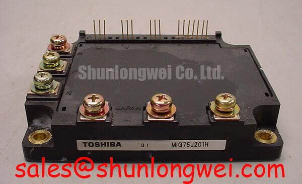
When a replacement module is installed in an industrial inverter welder or medium frequency induction heating supply, I first inspect the copper baseplate, heatsink contact surface, and mounting pattern before applying power. A slight convexity in the baseplate or a local high spot on the heatsink can concentrate mechanical stress through the thermal interface material and place the ceramic substrate under uneven loading. The Toshiba MIG75J201H is identified by an official voltage rating of 600.0 V, an official current rating of 75.0 A, and a Toshiba Intelligent Power Module package classification. These values establish the component identity and electrical rating class, while the final operating limits remain dependent on the complete converter design, thermal path, switching pattern, and protection system.
Place the heatsink on a clean, stable work surface and check its mounting face with a suitable flatness inspection method. Remove oxide, loose coating, old thermal compound, and embedded particles without scratching the contact area. The same inspection applies to the module baseplate. Do not use a mounting screw to force a visibly distorted surface into alignment. Such a procedure can create a mechanical load path through the ceramic rather than distributing pressure across the full baseplate.
For the thermal interface, apply a thin and continuous layer that covers the intended contact region without leaving dry islands or thick ridges. A 50 to 80 micrometre thermal interface layer is a general assembly design consideration, not an official MIG75J201H production specification. The correct thickness depends on the selected material, surface finish, contact pressure, and thermal resistance data supplied with that material. Engineers should confirm the final interface by checking contact transfer, mounting consistency, and temperature behavior during controlled commissioning.
Use a calibrated driver and tighten the mounting hardware progressively in a diagonal cross pattern. This distributes pressure while the interface settles and reduces the possibility of tilting the module against the heatsink. The fastening sequence, hardware grade, washer arrangement, and final torque should follow the applicable Toshiba documentation and the equipment manufacturer’s mechanical procedure. After installation, inspect the module edges for movement, tilt, or signs of baseplate distortion before connecting the power terminals.
Thermal troubleshooting should begin with temperature comparison across equivalent operating conditions. A rising case temperature, an abnormal difference between phase positions, or a temperature increase that follows a mounting change can point toward contact quality, airflow imbalance, switching loss, or load distribution. These observations do not identify one cause by themselves. Check the heatsink contact, fan direction, air path, electrical current balance, and switching waveform as separate evidence sources.
For preventive maintenance, remove accumulated dust from the heatsink and verify that the intended airflow reaches the module rather than bypassing it. Inspect thermal interface material for pump out, drying, contamination, or loss of contact after the equipment has experienced repeated thermal cycling. Maintenance Note: Monitor contact temperature during scheduled service and recheck the cooling path whenever dust loading, fan condition, or enclosure humidity changes.
Condensation deserves attention in equipment that moves between cold storage and a warmer production area. Keep the enclosure environment under control before energizing the power stage, and inspect terminal areas for moisture films or corrosion. The module rating does not by itself establish an enclosure’s condensation resistance, pollution degree, or insulation coordination. Those conditions must be evaluated at system level.
For engineers comparing possible repair references, MG75Q1ZS50 can be reviewed as a separate reference device. Its suitability cannot be assumed from current or voltage labels alone. Compare package geometry, terminal arrangement, internal control functions, electrical characteristics, thermal impedance, protection behavior, and gate drive requirements before considering any substitution.
Regenerative DC Bus Surge and Braking Energy Control
During motor deceleration, the first commissioning task is to trace where regenerative energy is routed from the motor into the DC bus and how the braking path is enabled. A braking IGBT and ballast resistor must be treated as a coordinated energy dissipation network, not as isolated parts selected only from the nominal bus voltage. The resistor must absorb the available deceleration energy without exceeding its pulse, thermal, insulation, or enclosure limits, while the switching device must remain within its voltage, current, temperature, and switching stress boundaries.
The 600.0 V official voltage rating of the MIG75J201H is a component rating reference. It does not define the allowable peak of a particular regenerative bus or guarantee immunity to overshoot generated by wiring inductance, commutation, control delay, or an incorrectly tuned braking threshold. During commissioning, record the DC bus waveform at the relevant switching node using measurement equipment and probing methods suitable for the transient environment. The system engineer should compare the measured peak and duration with the complete component and control documentation.
Braking resistor sizing should begin with the machine’s deceleration profile, rotating inertia, commanded speed change, duty repetition, and available cooling. The energy that reaches the resistor is determined by the mechanical system and control strategy, not by the 75.0 A official current rating alone. A resistor that survives a short bench pulse may still overheat under repeated production cycles. Review resistor pulse capability, average dissipation, mounting clearance, thermal radiation, and enclosure temperature as one design set.
When a braking transistor is placed inside a larger power module topology, trace the electrical path from the DC bus to the switching device and resistor. Minimize stray inductance in the high current loop according to the system layout objectives, then verify overshoot during actual switching conditions. Keep the control return path separate from the high current return path wherever the topology permits. This reduces the chance that load current transients will be interpreted as a control reference disturbance.
Complementary gate signals require a deliberate interlock strategy. The control board should prevent the upper and lower devices of the same switching leg from receiving overlapping drive commands, including during processor reset, brownout, fault recovery, and power sequencing. Dead time is a system determined parameter. Set it only after considering device turn off behavior, driver propagation mismatch, temperature variation, command delay, and the measured switching transition. Excessive dead time can increase diode conduction and switching loss, while insufficient dead time can create cross conduction.
At the bench, review the gate signal and the associated collector or switching node together. A clean logic command does not prove that the power device receives a clean gate waveform at its own reference terminal. Probe placement, common mode movement, driver isolation, and return inductance can alter the observed signal. Test startup, shutdown, repeated braking, fault reset, and the highest expected regenerative event rather than validating only a steady running condition.
Where the inverter welder or induction heating supply uses isolated control electronics, check the isolation barrier behavior during fast common mode voltage movement. Optical couplers and digital isolators have different propagation, supply, and common mode transient characteristics. The selected interface must be evaluated against the switching environment, board layout, and fault response requirements. The semiconductor module itself should not be described as independently certified for complete equipment EMC compliance. Compliance belongs to the assembled system and its applicable test configuration.
The engineering principles for gate drive arrangement, thermal paths, switching loops, and protection coordination are developed further in IGBT Design and Integration. Use that material to structure the review, then validate the actual repair assembly against its own schematic and measured waveforms.
Gate Loop Control, Emitter Referencing, and False Trigger Prevention
Before connecting a replacement drive board, identify every power and control terminal from the original circuit documentation and the module’s applicable pin assignment. Do not assume that a visually similar emitter connection has the same electrical function. In some power topologies, the main load emitter path and an auxiliary low inductance emitter return are treated differently by the driver. Whether the specific MIG75J201H configuration provides such an auxiliary connection must be confirmed from the applicable device documentation and board schematic.
The purpose of a dedicated driver return is to keep the gate voltage reference tied to the device control loop rather than allowing load current to modulate it. High di/dt in the main emitter path can produce a transient reference shift across shared copper and vias. The resulting gate to emitter disturbance may appear as an unwanted turn on, delayed turn off, oscillation, or an irregular switching edge. These symptoms require waveform correlation rather than a single-cause diagnosis.
Route the gate drive path as a compact forward and return loop. Keep the driver return close to the gate conductor, avoid unnecessary shared impedance with the power emitter path, and place the isolation and protection components according to the actual current loop. The control board should also maintain suitable clearance from high voltage copper, switching nodes, and resistor bodies. The required spacing is determined by working voltage, pollution conditions, insulation system, board material, and the applicable safety standard.
During troubleshooting, measure the gate to emitter voltage directly at the module terminals using a probe arrangement that does not introduce a long reference lead. Compare the command at the driver output with the voltage at the module. A difference between those observations may indicate loop inductance, common mode movement, return path coupling, or driver saturation. Inspect the signal during turn on, turn off, short pulse operation, fault response, and regenerative braking, because a stable low frequency command does not represent the complete switching environment.
Gate resistance, damping, negative bias, desaturation response, and soft shutdown are system design choices. They must be selected from the driver capability, module switching characteristics, thermal target, conducted noise limits, and measured transient margins. Avoid copying settings from another IPM solely because the voltage and current labels appear similar. The MIG75J201H should be commissioned with the gate drive arrangement specified for the actual module and converter topology.
False triggering can also originate outside the gate loop. Check digital isolator or optocoupler supply stability, control ground movement, connector contact quality, reset timing, and the behavior of the fault latch. In industrial inverter welders and medium frequency induction heating supplies, power stage noise can reach the control board through supply rails, shields, mounting hardware, and measurement cables. Separate these coupling paths during diagnosis, then confirm the correction under the highest practical switching stress.
For routine service, record the baseline gate waveform, DC bus behavior, heatsink temperature, and terminal condition after the equipment has passed commissioning. Future maintenance comparisons are more useful when the probe locations, load condition, ambient condition, and test sequence remain consistent. This approach supports controlled replacement decisions without treating the component’s official ratings as a substitute for complete system validation.