
Content last revised on September 16, 2026
N2500VC160 Ratings and Initial Commissioning Checks
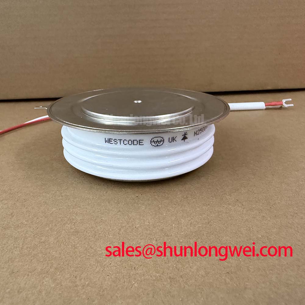
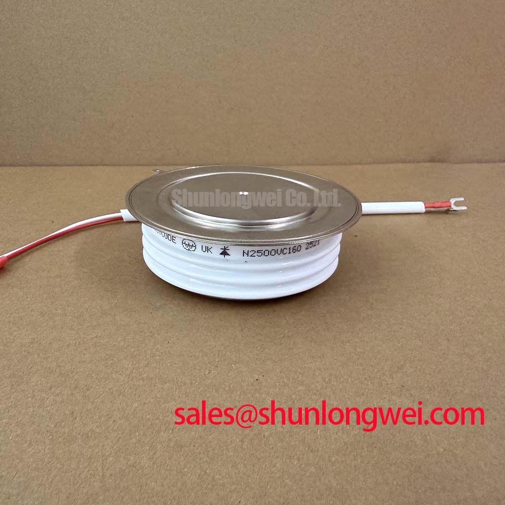
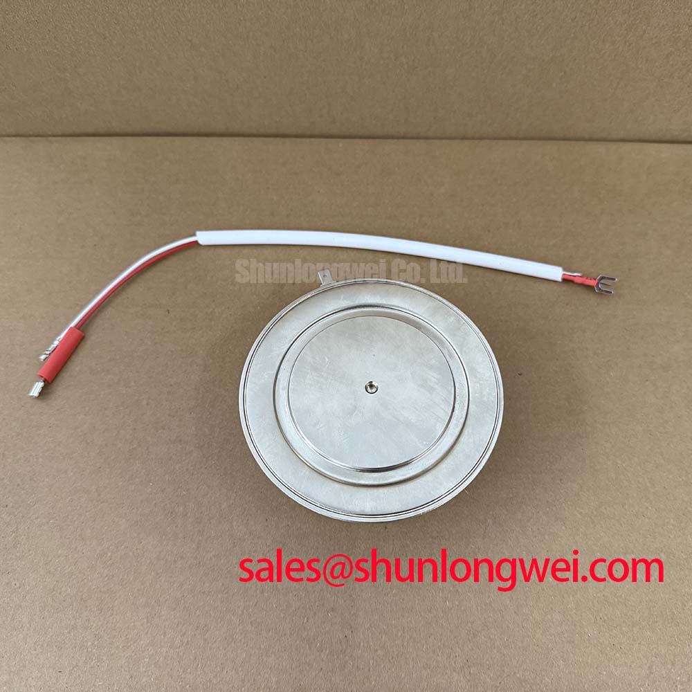
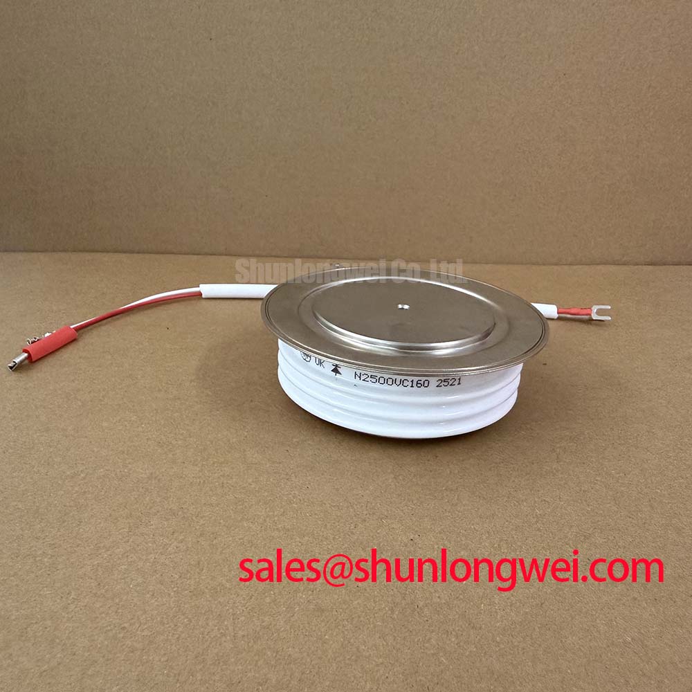
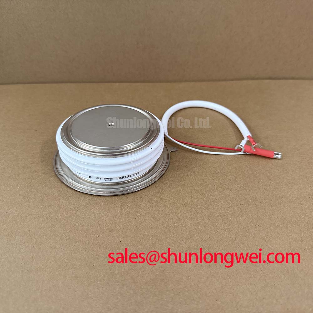
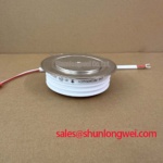
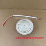
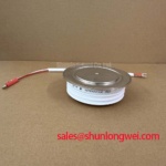
Before energizing a replacement, verify the Westcode nameplate, inspect the ceramic and terminal areas for mechanical damage, and compare the cold resistance readings with a known-good device from the same SVC assembly. The N2500VC160 is a high-current power diode specified for high-voltage industrial power conversion, including evaluation in grid-tied static var compensators and thyristor-switched capacitor banks.
| Parameter | Value | Classification |
|---|---|---|
| Repetitive peak off-state and reverse voltage, VDRM / VRRM | 1600 V | Official Specification |
| Mean on-state current, IT(AV) | 2500 A at Tsink = 55°C, double-side cooled | Official Specification |
| Peak non-repetitive surge current, ITSM | 37000 A at tp = 10 ms and Vrm = 0.6VRRM | Official Specification |
| Threshold voltage, V0 | 0.88 V | Official Specification |
| Junction-to-case thermal resistance, Rth(j-c) | 0.017 K/W, double-side cooled | Official Specification |
The current rating is inseparable from the stated cooling condition. A system engineer should therefore assess the complete thermal path, including contact surfaces, cooling hardware, busbar geometry, and operating waveform, rather than treating 2500 A as an unrestricted current value under every installation condition.
Field Diagnostics and Commissioning for the 10 ms Surge Current Rating
During SVC commissioning, the first electrical review should confirm that the applied repetitive off-state and reverse-voltage conditions remain within the applicable 1600 V VDRM and VRRM ratings. The listed 37000 A ITSM value is a peak non-repetitive surge specification at a 10 ms pulse duration and a reverse-voltage condition of 0.6VRRM. It should be used as a fault and transient evaluation boundary, not as a repetitive operating-current target.
For a thyristor-switched capacitor branch, record the actual current waveform during energization and compare its duration, peak value, and repetition pattern with the applicable protection study. A single half-cycle disturbance and repeated capacitor-bank switching impose different thermal recovery conditions. The junction temperature should be evaluated before reverse voltage is reapplied, especially where a protection event is followed by rapid branch commutation.
Fuse coordination requires the correct manufacturer data for the selected semiconductor fuse, including its I²t characteristic, clearing behavior, prospective fault current, and installation arrangement. The N2500VC160 rating alone does not establish a valid fuse selection. Designers should verify the fuse I²t coordination table against the complete SVC protection study and confirm that the fuse interruption profile is compatible with the diode’s permitted surge event.
Terminal inspection is equally important. Clean contact faces, even clamping pressure, correctly supported conductors, and low-inductance current paths reduce the chance that a healthy device will be exposed to abnormal local heating or switching overshoot. The approved terminal hardware and manufacturer-defined mounting torque must be taken from the applicable Westcode mechanical documentation; a generic torque value should not be substituted for the device-specific requirement.
For procurement and maintenance records, document the voltage class, current class, cooling arrangement, fuse reference, installation position, and measured pre-commissioning condition. The 6RI75G-160B may be reviewed as a separate same-category reference during compatibility analysis, but its mechanical and electrical interchangeability must be verified independently.
RC Snubber and Commutation Layout Considerations
An RC snubber across a high-power diode or its switching branch is a system-level protection network. Its purpose may include controlling voltage-rate transients, reducing ringing, and limiting the possibility of unintended behavior in adjacent thyristor devices. The correct resistor and capacitor values depend on the measured stray inductance, switching waveform, capacitor-bank topology, damping requirements, and the characteristics of the connected semiconductor stack.
For the N2500VC160, begin with oscilloscope measurements taken at the device terminals using a suitable high-voltage differential probe and a current measurement method appropriate for the branch. Look for voltage overshoot, ringing frequency, repetitive transient amplitude, and changes in waveform when the snubber is connected. The design objective is to minimize parasitic loop inductance and suppress excessive switching stress, while the final network values remain determined by the complete power circuit and verified through switching tests.
A saturable reactor may also be evaluated where the capacitor-bank inrush or commutation current produces an excessive di/dt. Its selection should account for prospective fault current, pulse duration, reset behavior, and the repetitive operating profile of the SVC. The N2500VC160 datasheet ratings do not specify a universal reactor value or snubber setting, so these components require system calculation and laboratory validation.
Keep the snubber loop physically compact and avoid routing its conductors beside sensitive gate, firing, or measurement wiring. The current return path should be intentional, with the busbar arrangement reviewed for symmetry. If the switching transient changes substantially between a bench test and the installed cabinet, investigate conductor length, mounting contact, cabinet bonding, and measurement-loop influence before changing the protection network.
Although display technologies are electrically separate from this power device, engineers responsible for combined power-control and monitoring cabinets can consult references on MicroLED flat-panel technology and OLED active-matrix displays when assessing control-panel architecture. Those display references do not define the N2500VC160 electrical limits or establish EMC compliance for the completed SVC equipment.
💡 Pro Tip: Use a symmetrical busbar layout where practical, then verify turn-off overshoot and peak-voltage margin with a properly isolated oscilloscope during double-pulse or equivalent switching tests.
Thermal Interface Evaluation Across the Double-Side Cooling Path
The stated Rth(j-c) of 0.017 K/W applies to the specified double-side-cooled condition. This value is an official thermal specification for the junction-to-case path; it is not the thermal resistance of the complete assembly. Heatsink flatness, contact pressure, thermal interface material distribution, coolant or airflow performance, and the actual current waveform all influence the resulting junction temperature.
Before installation, inspect both mating surfaces for contamination, burrs, scratches, or distortion. The interface material should be spread evenly according to the thermal compound manufacturer’s process instructions. Excess material can increase mechanical displacement and contamination risk, while insufficient coverage can leave localized air pockets. The suitable application thickness is system- and material-dependent and should be established by the approved assembly procedure rather than guessed from the semiconductor rating.
Double-side cooling requires controlled mechanical parallelism. Tightening one side completely before the opposite side can create uneven pressure and local stress. Use the approved sequence, hardware, washers, and torque specification from the mechanical drawing associated with the device assembly. After clamping, inspect for evidence of rocking, extrusion, or incomplete contact and retain the assembly record for maintenance traceability.
Thermal verification should use the actual SVC duty cycle, including capacitor switching intervals, fault recovery events, ambient conditions, and cabinet cooling behavior. The 2500 A IT(AV) rating at Tsink = 55°C is conditional on double-side cooling and should not be transferred directly to a single-side arrangement. If the measured case temperature or temperature rise differs from the thermal model, check the interface and clamping process before attributing the result to semiconductor variation.
Transient thermal behavior also matters. A short surge can produce a different junction-temperature response from a sustained current interval because the thermal impedance changes with pulse duration. The engineering calculation should use the applicable transient thermal impedance data from the complete manufacturer documentation, together with the real current waveform and initial case temperature. No lifetime or field-failure conclusion should be drawn without controlled test data and an identified technical source.
Reverse-Voltage Recovery and Protection Review in High-Current Branches
The N2500VC160 is identified here by its reverse-voltage and high-current diode ratings, but the supplied parameter set does not provide diode reverse-recovery charge, peak reverse-recovery current, recovery time, or a soft-recovery classification. Those values must be confirmed from the applicable manufacturer datasheet before engineers calculate commutation loss, EMI behavior, or snubber dissipation for a specific circuit.
In an SVC branch, reverse recovery can interact with transformer leakage inductance, busbar stray inductance, capacitor-bank impedance, and the firing sequence of neighboring thyristors. During commissioning, capture both the diode voltage and branch current at the semiconductor terminals. Compare the observed recovery event with the validated simulation model and the known-good phase position. An unexpected spike may indicate layout inductance, probe error, timing interaction, or component stress; it should not be assigned to one cause without waveform evidence.
Protection review should include the maximum repetitive reverse voltage, temporary overvoltage behavior, fuse clearing sequence, and the timing of reverse-voltage reapplication after a surge event. The 1600 V VDRM / VRRM rating is an official component boundary, while cabinet-level insulation coordination, clearance, creepage, and EMC performance remain responsibilities of the completed equipment design.
Where gate-controlled devices operate alongside the diode, firing and commutation circuits should be checked for unintended coupling during high dv/dt events. The reference Evolution of Negative Off-Bias Gate Drive Circuits can support an engineering review of gate-control practices for adjacent thyristor systems. It does not add an unstated gate-drive requirement to the N2500VC160 and should not be treated as a substitute for the relevant device and system documentation.
For final acceptance, verify the reverse-voltage waveform, surge-current event, thermal interface condition, fuse coordination, and terminal assembly against the project’s approved limits. Record the test conditions, probe locations, cooling configuration, and switching sequence so that future maintenance teams can compare the installed branch with its commissioned baseline.