Content last revised on September 15, 2026
Benchtop Waveform Tuning: Mitigating Stress via Transient Thermal Impedance on PM300DSA120
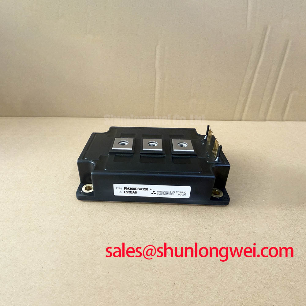
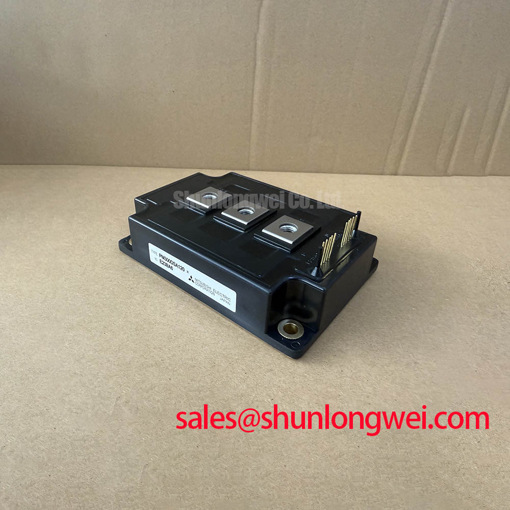
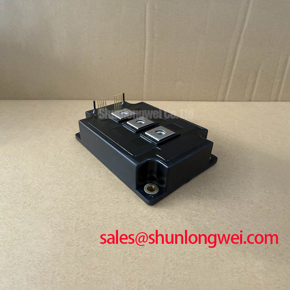
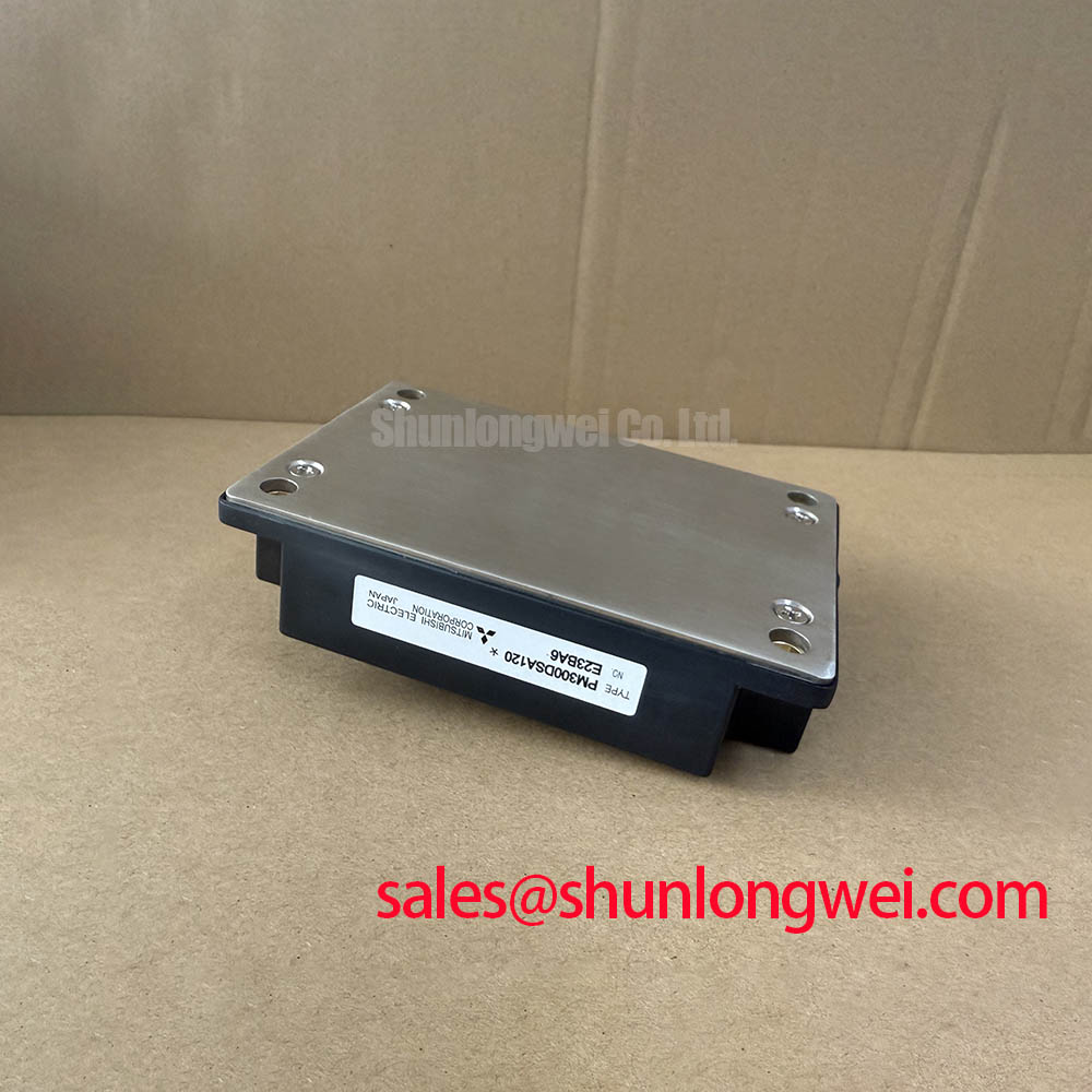
With the DC link discharged and isolated, first verify the PM300DSA120 terminal arrangement against the original equipment documentation, inspect the module baseplate and terminal areas for distortion or heat marking, and compare the installed controller’s protection wiring before applying gate drive power.
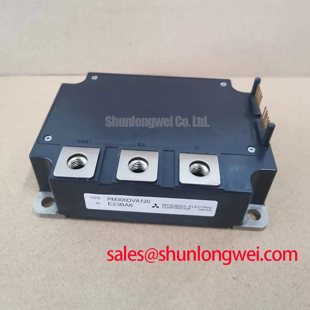
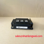
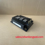
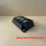
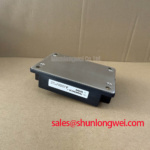
The PM300DSA120 from Mitsubishi Electric is a high current power module rated at VCES = 1200 V and IC = 300 A at TC = 25°C, according to the official specification. Its specified pulsed collector current is 600 A for a transient pulse width of 1 ms or less. The module is relevant to inverter and power conversion assemblies where the existing electrical topology, gate driver interface, heat sink arrangement, and protection logic have all been verified by the system integrator.
| Official Specification | Value | Condition |
|---|---|---|
| Collector emitter voltage, VCES | 1200 V | Datasheet test conditions apply |
| Continuous collector current, IC | 300 A | TC = 25°C |
| Peak collector current, ICP | 600 A | Pulse width not exceeding 1 ms |
| Maximum collector dissipation, PC | 1790 W | TC = 25°C, per module element |
| Junction to case thermal resistance, Rth(j c)Q | 0.07°C/W maximum | Each IGBT |
| Over temperature protection trip, OT | 110°C typical | 100°C minimum threshold |
| Isolation voltage, Viso | 2500 Vrms | AC, 1 minute, 60 Hz sinusoidal |
For a repair bench or a controlled recommissioning test, the continuous 300 A rating should not be treated as a direct allowance for repetitive overload operation. It is specified at TC = 25°C, while a working inverter experiences heat sink temperature variation, switching loss, conduction loss, cooling air contamination, and load duty changes. The stated 1790 W maximum collector dissipation is also an official limit at the same case temperature condition, per module element, rather than a prediction of usable dissipation in a closed industrial cabinet.
The official maximum junction to case thermal resistance of 0.07°C/W for each IGBT establishes the steady thermal path from junction to the case. During a pulse event, junction temperature does not immediately follow the steady state resistance because the thermal mass of the silicon, internal assembly, baseplate, interface material, and heat sink responds over different time periods. A multi RC thermal impedance model is the appropriate Engineering Calculation method where the manufacturer’s transient thermal curves are available for the exact module revision. The system engineer can combine measured loss energy, pulse duration, repetition rate, measured case temperature, and the applicable transient impedance curve to assess junction temperature margin.
On the bench, capture collector emitter voltage, collector current, gate voltage, DC bus voltage, and case temperature together. A current pulse that appears acceptable in one switching cycle can still create excessive average heating when repeated under a real traction duty cycle. If the waveform shows an elevated current tail, abnormal collector voltage overshoot, or inconsistent switching intervals, pause testing and verify gate drive timing, current measurement bandwidth, DC link capacitor placement, and thermal contact before attributing the result to the module.
The module’s specified over temperature protection trip is 110°C typical, with a 100°C minimum threshold. This protection value should be treated as an official protective threshold, not as a preferred continuous thermal operating target. Designers should verify how the host equipment interprets the temperature signal, whether a fault latch is present, and whether restart is inhibited until the heat sink and module case have stabilized.
For electric material handling and forklift low voltage traction equipment, this module can be evaluated only after confirming the inverter bus voltage, motor current profile, protection thresholds, and cooling capacity of the original drive. Repeated acceleration, ramp climbing, hydraulic pump demand, and regenerative events can create a duty cycle that differs substantially from a static current test.
⚠️ Maintenance Note: Periodically monitor terminal and heat sink contact temperature rise, clear blocked cooling paths, and inspect aged thermal interface material before it compromises heat transfer.
Thermal Interface Material Thickness for PM300DSA120
The thermal interface between the PM300DSA120 baseplate and heat sink deserves the same inspection discipline as the power terminals. A controlled, thin and uniform thermal interface material layer helps reduce contact resistance while accommodating practical surface variation. The appropriate thermal interface thickness is a General Industry Design Consideration, not a Mitsubishi Electric module specification. The correct material, application method, and final thickness must be verified against the inverter manufacturer’s service documentation and the characteristics of the selected heat sink.
Before fitting the module, clean the mating surface without leaving fibers, hardened compound residue, or debris around mounting holes. Use a controlled application method that avoids isolated high spots and air voids. Baseplate flatness, heat sink flatness, and fixture condition all influence the final contact pattern. A module that is electrically functional can still develop a local thermal problem when mechanical loading is uneven across its mounting plane.
Sequential tightening is a Design Consideration that helps distribute pressure gradually across the baseplate. Follow the original equipment’s specified fastener type, sequence, and tightening torque. Do not substitute a general mounting torque as an official requirement for this model. After the first thermal run, a maintenance team should inspect for evidence of compound migration, loosening hardware, restricted airflow, or condensate paths that can reach the heat sink and terminal area.
Where several power modules operate in parallel, static current balance depends on the device electrical characteristics, temperature distribution, gate drive consistency, and symmetry of the conductor path. The temperature behavior of VCE(sat) can contribute to sharing behavior, but it does not remove the need for measured verification. Keep corresponding busbar paths physically symmetric where practical, ensure comparable heat rejection between positions, and measure current distribution under controlled load conditions.
In a system requiring a different module architecture, engineers may compare topology, ratings, terminals, driver compatibility, thermal interface, and protection behavior with products such as SKIIP37AC12T4V1. This is a neutral technical comparison point, not a declaration of direct interchangeability.
PM300DSA120 Circuit Protection & Reliability: Calibrating DC Bus Low Inductance Laminated Busbar Design
At turn off, the voltage presented to a power switch can rise above the DC link level because stray loop inductance interacts with the rate of current change. In Engineering Calculation terms, the additional transient contribution follows the relationship of DC bus voltage plus loop inductance multiplied by current slew rate. The actual peak must be measured at the module terminals with a suitably rated, low loop measurement method; it cannot be established reliably from a schematic alone.
A laminated or closely coupled busbar is a Design Consideration for minimizing the high current commutation loop inductance. The relevant condition is suppression of turn off overshoot and ringing while maintaining the electrical clearances, mechanical strength, insulation system, and service access required by the equipment. The system engineer should validate peak voltage margin against the DC link voltage during switching tests across the expected load and temperature range.
Place the DC link capacitor system so that the switching current loop is compact, then inspect the physical current path rather than relying only on PCB artwork. Long leads, unnecessary bends, loosely supported conductors, and separated positive and negative paths can increase parasitic inductance. Snubber capacitor selection must be based on measured ringing frequency, stored energy, capacitor ripple capability, thermal performance, and the operating limits of the complete inverter. There is no universal capacitance value that can be safely assigned to the PM300DSA120 without those system measurements.
If the inverter includes an input rectifier or auxiliary power stage, its behavior should also be checked during abnormal bus events. A related module such as CM300DXDX1-24A may be reviewed when documenting the front end or complementary rectification stage. Mitsubishi Electric also publishes a diode modules lineup that can help engineers distinguish power diode module categories when checking a system bill of materials.
For troubleshooting, inspect the capacitor bank connections, busbar fasteners, insulation barriers, and mounting supports before increasing test voltage or current. A ringing waveform may result from bus geometry, probing arrangement, capacitor degradation, driver timing, or a combination of factors. Compare the result against a known stable inverter channel where available.
PM300DSA120 Circuit Protection & Reliability: Optimizing Gate Drive Loop Geometry to Prevent Oscillation
Gate loop geometry should be reviewed separately from the main power loop. Shared high current return paths can introduce voltage disturbance into the gate reference during switching. That disturbance may alter the apparent gate emitter voltage seen by the IGBT, producing unwanted switching behavior or oscillation. The system design objective is to keep the gate drive return path controlled and to avoid coupling it unnecessarily to the main high current emitter path.
Do not assume an auxiliary emitter arrangement, gate terminal convention, or internal sensing connection from a generic module family description. The service engineer should verify the terminal designation and gate driver connection directly from the original PM300DSA120 equipment documentation. During diagnosis, inspect the gate resistor network, driver connector seating, isolation barriers, return conductors, and any active clamp circuitry fitted by the inverter manufacturer.
The Miller region deserves oscilloscope attention when collector voltage changes rapidly. Gate voltage movement during that interval can be influenced by gate loop inductance, drive impedance, collector gate capacitance behavior, and common mode disturbance. An active clamp, if included in the host driver design, must be evaluated as part of the complete protection sequence rather than as an independent replacement part. Designers should verify turn on and turn off waveforms under the relevant DC bus and load conditions, then confirm that protection timing remains coordinated with the controller fault response.
Humidity and condensation control are practical maintenance concerns around traction and warehouse equipment, especially where a cold vehicle enters a warmer service area. Keep enclosure seals, cable glands, blower paths, and control board surfaces under inspection. Before return to service, confirm that insulation, terminal hardware, gate connections, and cooling airflow are dry and mechanically secure. For broader test planning and power module reliability topics, consult the Power Electronics Masterclass.