



Content last revised on September 19, 2026
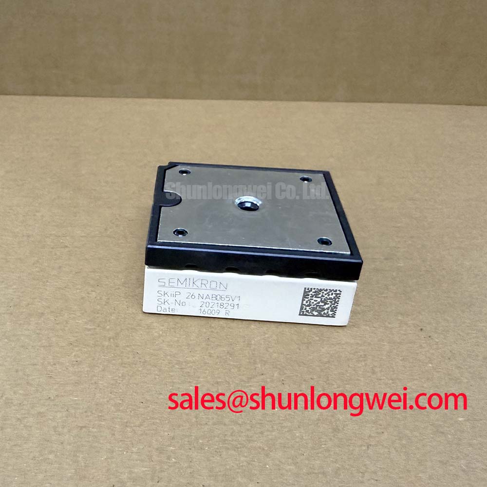
SKIIP 26NAB065V1 Specifications and Initial Inspection
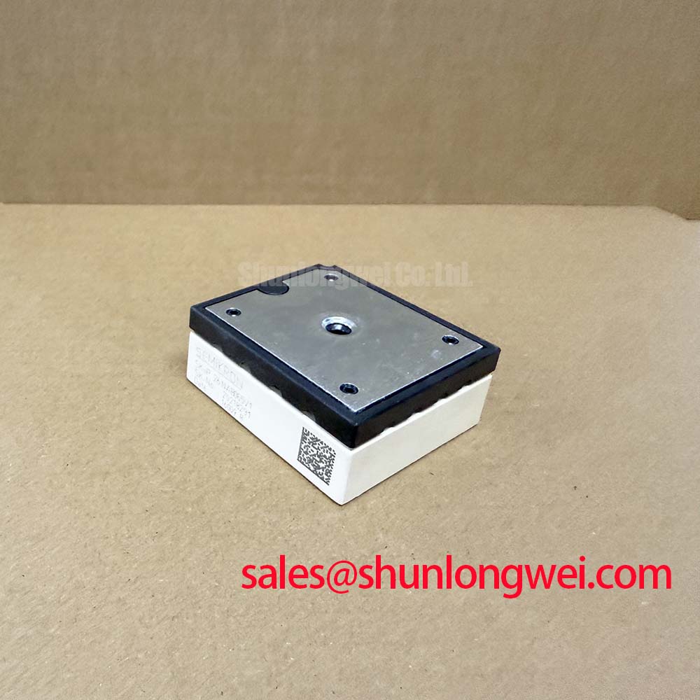
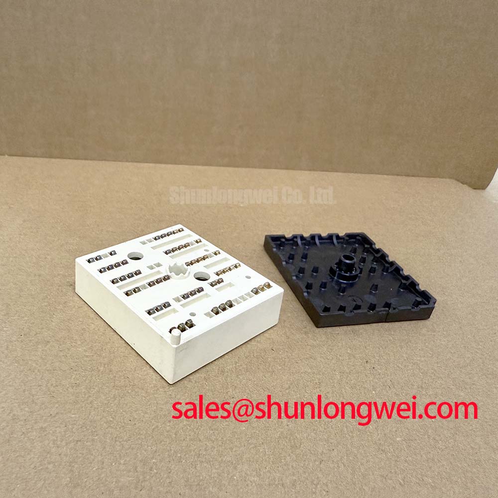
With the drive isolated and the DC link discharged, begin by checking the module body, mounting interface, power terminals, and control connector for heat discoloration, cracked plastic, loosened hardware, or residue before taking cold-state resistance readings. The SKIIP 26NAB065V1 is a Semikron power module rated at 600 V VCES, with 35 A continuous DC collector current at Tj = 175°C and 50 A nominal collector current as Official Datasheet Specifications. Its stated operating junction-temperature range is −40°C to +150°C.
| Official Datasheet Specification | Value |
|---|---|
| Collector-emitter voltage, VCES | 600 V |
| Continuous DC collector current at Tj = 175°C, IC | 35 A |
| Nominal collector current, ICnom | 50 A |
| Collector-emitter saturation voltage at IC = 50 A, Tj = 25°C | 1.8 V typical, 2.2 V maximum |
| Junction-to-case thermal resistance per IGBT | 1.4 K/W |
| Repetitive peak reverse voltage, VRRM | 1600 V |
| Forward current at Tcase = 80°C, IFAV | 35 A |
| Junction-to-case thermal resistance per diode | 1.8 K/W |
| Insulation test voltage, RMS, 50 Hz, 1 minute, Visol | 2500 V |
| Operating junction temperature, Tj(op) | −40°C to +150°C |
SKIIP 26NAB065V1 Circuit Protection & Reliability: Symmetrical Busbar Geometry for High Current
In a compact industrial inverter or high-speed CNC spindle drive, start compatibility work by matching the original circuit function, mechanical footprint, terminal arrangement, gate-drive interface, cooling path, and protection architecture. Voltage and current ratings alone do not establish interchangeability. The 600 V VCES rating and 35 A continuous-current rating provide the electrical identity of this module, while the complete assembly must still be checked against the original equipment documentation.
Design Consideration: where parallel current paths exist in the surrounding converter, physical symmetry matters. Equal-length busbar routes, comparable conductor cross-sections, and matched gate-loop routing help prevent one path from seeing substantially different parasitic inductance or resistance. The positive temperature behavior associated with IGBT conduction can support steady-state sharing under controlled conditions, but it does not correct unequal switching-loop geometry. Dynamic imbalance is normally revealed on a differential measurement of switching voltage and current, rather than by a static multimeter reading alone.
For field triage, compare the failed assembly against a known-good channel where available. Look for unequal terminal heating, busbar witness marks, distorted lugs, or uneven thermal-interface contact. A cold resistance check can identify a clear short circuit, but it cannot validate switching behavior, gate-drive timing, or insulation performance under operating voltage. The 2500 V RMS insulation test rating for 1 minute at 50 Hz is an Official Datasheet Specification, not an instruction to apply an arbitrary field test voltage.
⚠️ Field Alert: Tighten hardware only to the equipment and module mounting documentation, and keep the thermal interface clean and uniformly applied before energizing the drive.
When an alternative module is being evaluated during a repair assessment, SKIIP37AC12T4V1 should be reviewed as a separate engineering candidate rather than assumed to be a direct replacement; its electrical ratings, control connections, package geometry, and protection behavior require verification in the actual equipment.
SKIIP 26NAB065V1 Circuit Protection & Reliability: Turn-Off di/dt and Peak-Voltage Control
Turn-off stress must be assessed at the installed DC-link voltage and actual load current. Engineering Calculation: the observed peak collector-emitter voltage follows the relationship of DC-link voltage plus stray-loop inductance multiplied by turn-off current slew rate. This is why the physical distance between the DC-link capacitor, busbars, and module terminals has a direct effect on overshoot. Minimize loop inductance to suppress inductive voltage rise, then verify peak margins against the DC-link voltage with properly rated differential probes during switching tests.
The official 1.8 V typical and 2.2 V maximum VCE(sat), specified at 50 A and 25°C, describes conduction behavior only at those stated conditions. It should not be used as a complete loss estimate for a spindle drive. Switching frequency, DC-link voltage, gate-drive behavior, load current waveform, cooling conditions, and commutation events all contribute to installed power dissipation. The stated junction-to-case thermal resistance of 1.4 K/W per IGBT and 1.8 K/W per diode gives the official thermal path values, while the heatsink and airflow remain system-determined.
Design Consideration: a snubber network or DC-link capacitor arrangement should be evaluated from measured ringing frequency, overshoot, capacitor ripple capability, and the available installation space. Do not select suppression components from a generic value. In regenerative braking operation, the braking chopper, braking resistor, DC-link capacitor condition, and control threshold should be checked as a group. A brake resistor absorbs regenerated energy only when the surrounding control circuit commands it; a module replacement does not correct a failed braking-control path.
The diode section is specified with 1600 V VRRM and 35 A IFAV at Tcase = 80°C. These official ratings should be interpreted with the original converter topology and commutation path. Engineers assessing higher switching-speed power stages can consult The 1200 V CoolSiC™ MOSFET Advantage in Three for broader three-phase conversion context; it does not alter the ratings of the SKIIP 26NAB065V1.
SKIIP 26NAB065V1 Thermal-Electrical Optimization: High-Speed Fault Management and VCE Desaturation
A healthy gate-drive circuit should be checked before condemning the IPM. With power removed, inspect the driver supply rails, gate resistor path, desaturation sensing components, isolated control wiring, and fault-return connection. Under controlled commissioning, compare the command waveform, gate waveform, collector-emitter waveform, and fault signal with a known-good channel or the equipment service reference. A persistent fault may reflect a module condition, but it can also arise from a driver supply collapse, incorrect enable sequence, damaged sensing network, or load-side fault.
Design Consideration: desaturation protection should identify abnormal collector-emitter behavior early enough for the controller’s documented short-circuit protection sequence. A two-stage turn-off strategy is often evaluated because an abrupt gate removal during a fault can create severe inductive overshoot. Its blanking interval, threshold, discharge path, and soft-turn-off behavior are controller-specific and must be validated against the installed busbar inductance, DC-link condition, and motor or spindle load.
Negative gate bias is also a system-level decision, not an official specification stated for this module. Where the original driver uses negative turn-off bias, preserve the original driver architecture and verify that the gate-emitter voltage remains within the module and driver limits during common-mode transients. Changing bias polarity or resistor values without waveform testing can create oscillation, delayed turn-off, or an unsuitable protection response.
For package and technology context, Semikron provides information on MiniSKiiP® power modules and its sintering technology. These resources support general evaluation of power-module packaging approaches and should not be treated as confirmation of unlisted construction details for this specific model.
Transient Dynamics & Electrical Design: Auxiliary Emitter Return Trace Separation on SKIIP 26NAB065V1
Common-mode noise often enters a drive through shared return paths rather than through the logic command itself. Keep the gate-driver reference return separate from the high-current emitter return wherever the original module and drive layout provide distinct connections. This Design Consideration reduces mutual coupling between power current and the gate-control reference, helping the driver measure the intended gate-emitter condition during rapid switching.
During an on-site repair, inspect connector retention, return-path continuity, shield termination, and the physical route of low-level control wiring. If switching oscillation or unexplained overcurrent protection appears after replacement, do not assume a single cause. Verify the gate waveform at the relevant device reference, inspect the DC-link connection for looseness, and compare signal routing with the original layout. Long temporary leads, poorly placed probe grounds, and a changed return path can all distort the observed result.
For compact inverter and high-speed CNC spindle-drive integration, retain the original separation between high-energy power conductors and control wiring, then validate operation progressively under the equipment’s approved commissioning process. The final acceptance decision should be based on measured voltage stress, current balance, thermal behavior, fault response, and the host system’s documented electrical limits.