
Content last revised on October 2, 2026
SKKE600F12 Electrical Identity and Thermal Integration
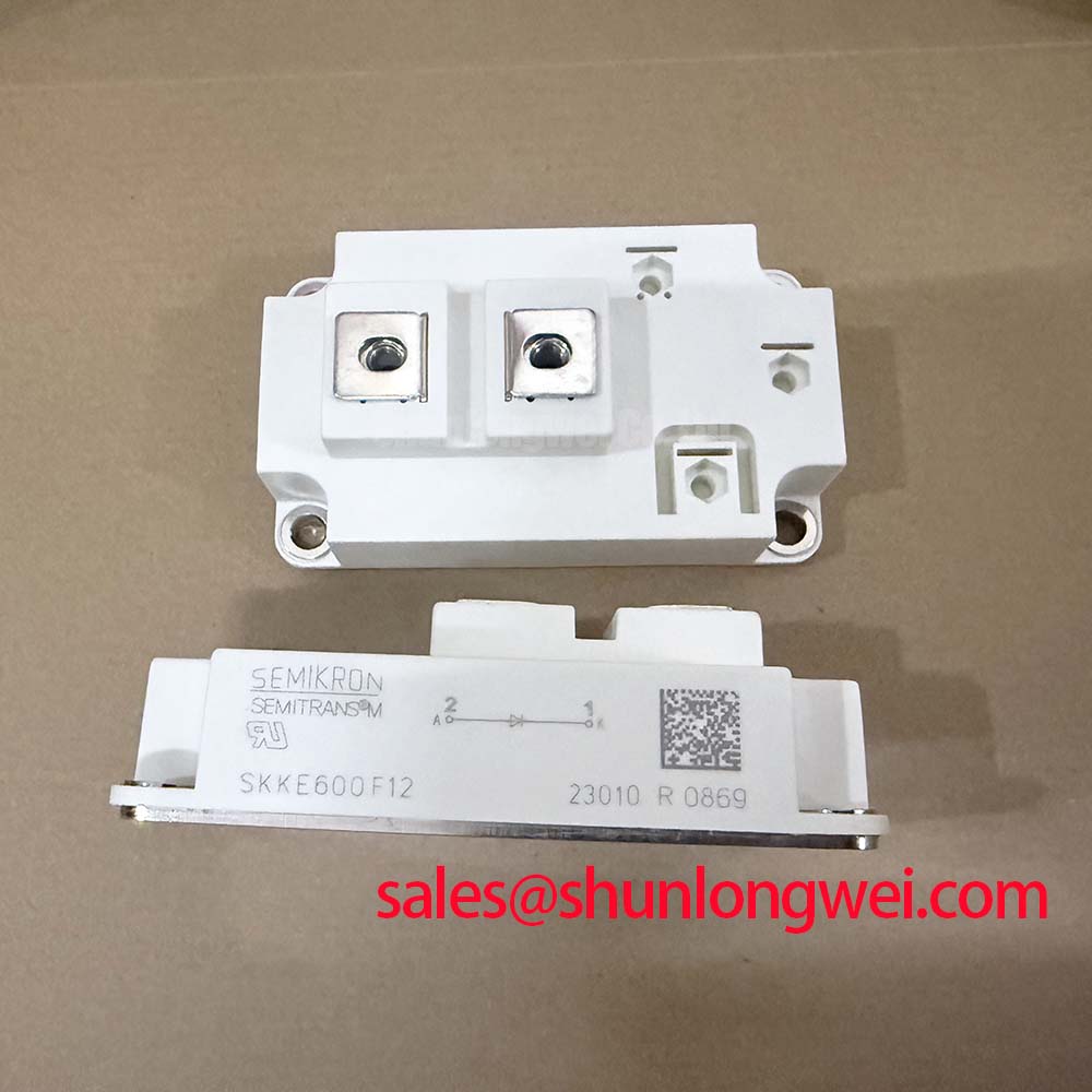
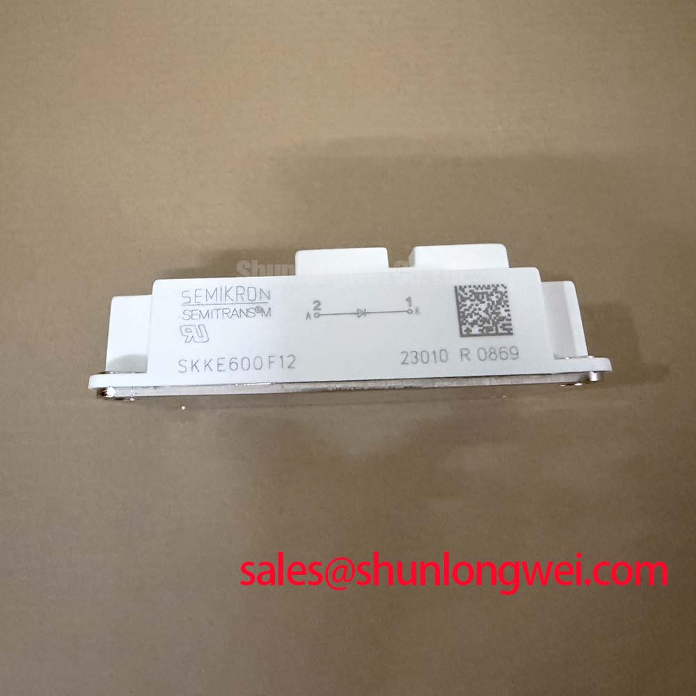
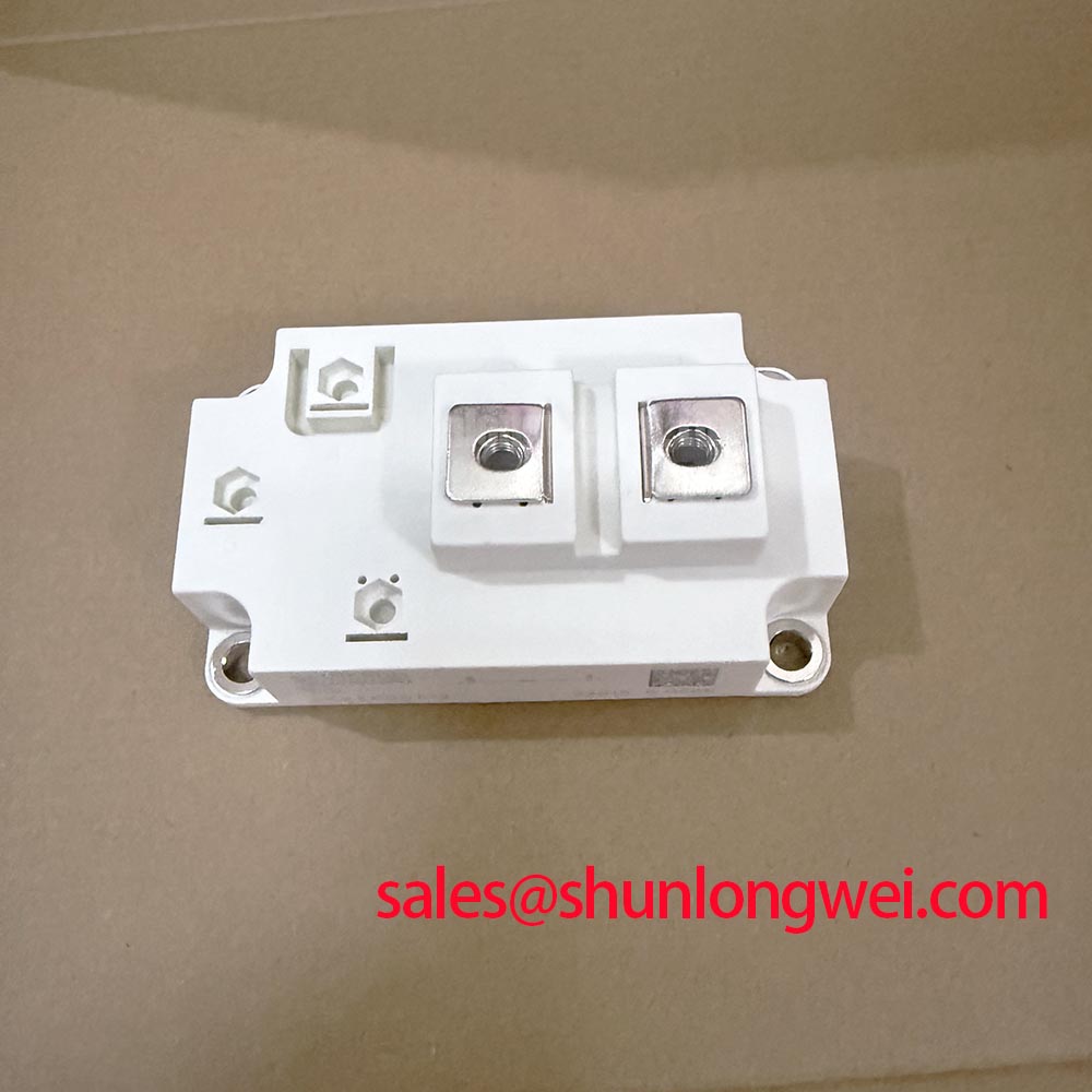
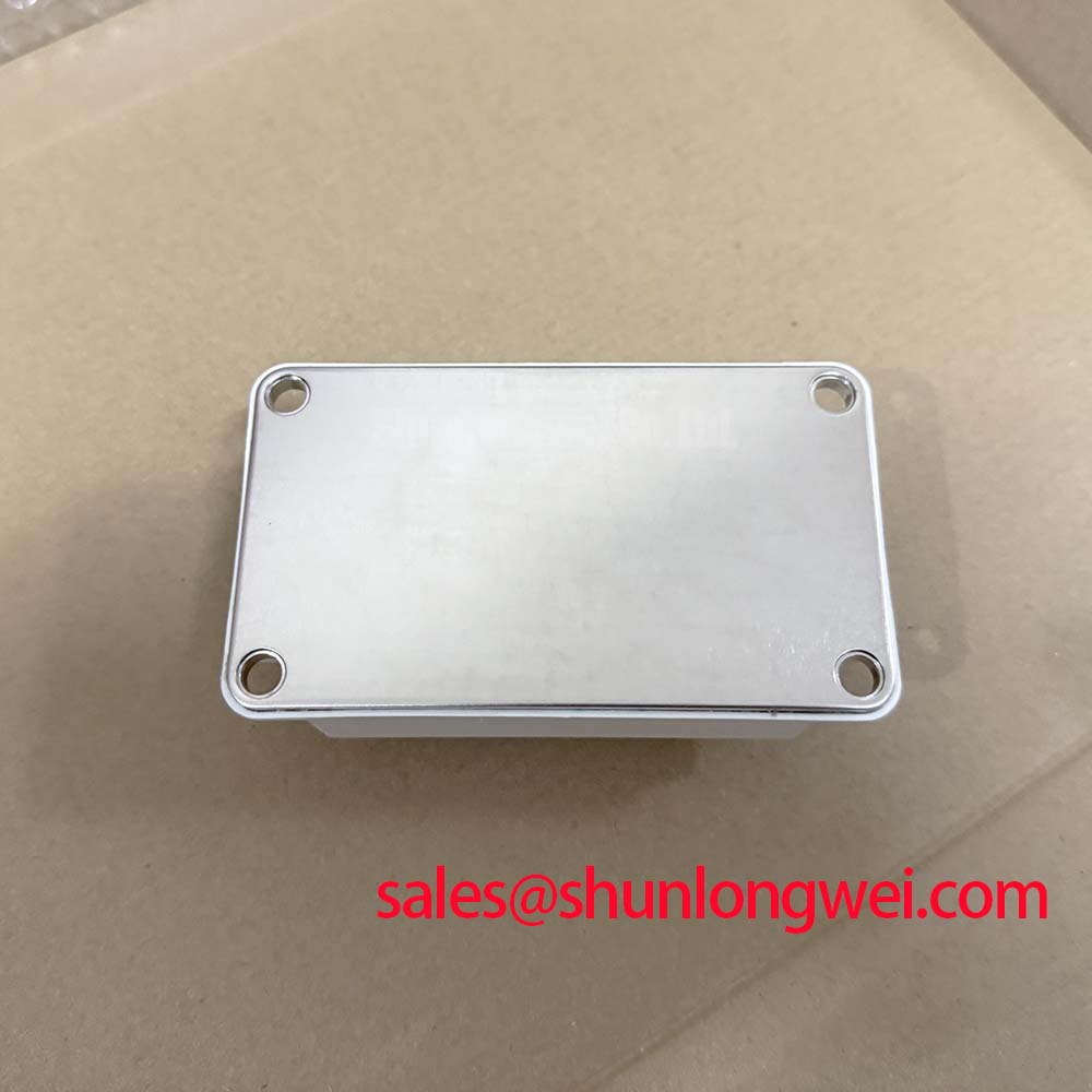
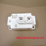
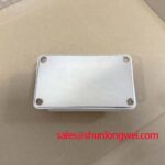
Begin a replacement inspection by checking the nameplate, package condition, terminal integrity, and the original system documentation before applying power. The Semikron SKKE600F12 is a diode module with a specified voltage rating of 1200 V and a rated current of 600 A under the applicable datasheet conditions. Surge current capability, thermal resistance, dimensions, and mounting details should be verified from the applicable manufacturer documentation before design release.
For a heavy duty variable frequency AC motor drive, the surrounding power stage determines the actual electrical and thermal stress. Designers should verify the DC link voltage, switching sequence, motor cable arrangement, short circuit protection, and cooling capacity against the module’s approved operating limits. A copper busbar arrangement with short, symmetrical current paths is a practical design consideration because it reduces unwanted commutation voltage and improves measurement repeatability.
When several semiconductor paths operate in parallel, differences in forward voltage and temperature can affect current sharing. Balanced dynamic current during switching is not automatic. Matching power loop geometry and the timing and layout of associated switches remains necessary. If current probes show unequal pulses, inspect the physical loop arrangement and switching sequence before attributing the issue to the module itself.
A MOV can be evaluated as part of the drive’s overvoltage absorption network, while an RC snubber may address faster switching transients close to the commutation path. The MOV voltage rating, energy capability, leakage behavior, and coordination with upstream protection are system design matters. They should be selected from measured surge conditions rather than treated as fixed properties of the SKKE600F12.
Transient Dynamics and Electrical Design for Atmospheric Exposure
Atmospheric neutron effects and altitude require application specific reliability data. No FIT value, altitude derating curve, or operating lifetime figure is established here as an official parameter for the SKKE600F12. Engineers evaluating equipment above normal installation elevations should obtain qualified semiconductor reliability data and compare it with the actual DC bus, switching waveform, enclosure environment, and operating profile.
Phase angle control and line frequency ripple smoothing can influence the voltage and current conditions presented to the inverter DC link. During commissioning, record the bus waveform under acceleration, deceleration, regeneration, and abnormal load transitions. A scope trace taken at the module terminals is more useful than a calculated nominal value alone because wiring inductance, braking hardware, and motor cable behavior can alter the transient.
RC snubber networks and MOV assemblies should be coordinated with the measured switching waveform. Excessive capacitance can increase switching current, while insufficient damping may leave high frequency ringing near the module terminals. The correct values are determined by the complete power topology and verified through controlled switching tests. The Semikron Danfoss SKiiP technology reference provides useful industry context for power semiconductor integration, but it should not be treated as a specification for this exact part.
Gate Voltage Spikes in Associated Switches and Commissioning Checks
In an associated IGBT switch, high dv/dt can couple through device capacitances and raise the gate voltage while the switch is inactive. This can contribute to unwanted cross conduction, but the measured cause must be established from the actual gate emitter waveform. Use a properly rated differential probe, observe both switching positions, and compare the signal with a known good phase leg. Inspect gate resistor placement, driver return routing, isolation integrity, and the distance between power and control conductors.
An active Miller clamp may be considered when the associated gate driver and switch topology support it. Negative gate bias is also a system design option for the switch, not a requirement of the SKKE600F12 diode module. The integrator should verify the switch’s permitted gate voltage range, driver output capability, isolation behavior, and turn off margin from the correct documentation before applying any negative bias.
During a failed start up, isolate the DC link and follow the site discharge procedure before touching the power stage. Check the associated switch’s gate to emitter impedance, inspect the driver supply under load, and confirm that protection timing is consistent across all phases. A gate waveform that differs from the other legs may indicate a wiring, driver, probe, or switch condition and requires controlled comparison rather than a single cause assumption.
For maintenance planning, the Field Engineer’s Handbook offers broader guidance on testing, failure analysis, and reliability evaluation. It is complementary engineering reference material, not a substitute for the SKKE600F12 manufacturer data.
Commutation Loop Inductance, Surge Current, and Mechanical Service
Turn off overshoot is governed by the interaction between DC link voltage, commutation loop inductance, switching current slope, and the installed clamp network. The relationship can be used as an engineering calculation, but the resulting peak must be confirmed with a low inductance voltage probing method at the module terminals. Designers should minimize parasitic loop area and use a symmetrical planar busbar arrangement where practical, then verify peak voltage margins during switching tests.
The module’s ITSM surge current rating and recovery limits must come from the applicable official datasheet. Do not infer surge capability from the 600 A rated current. Repeated overloads, short circuit events, and elevated junction temperature can reduce the available thermal recovery window. Protection coordination should therefore be validated using the actual fuse, gate driver for associated switches, current sensor, DC link, and cooling system.
Thermal service also depends on the module-to-heatsink interface. Remove aged thermal interface material, clean both mating surfaces, and apply a uniform layer according to the selected compound supplier’s instructions. The correct bolt pattern and tightening torque must be taken from the module mechanical documentation and the heatsink assembly specification rather than copied from a generic hardware table. Maintenance Note: Monitor contact temperature during scheduled inspections and verify that the heatsink airflow remains unobstructed.
For a field replacement assessment, compare the original electrical topology, terminal arrangement, cooling method, and protection circuit. A replacement review should remain conditional on verified ratings, footprint, electrical behavior, and system test results; an IGBT module such as SKM100GB063D is not a direct substitute for the SKKE600F12 diode module.