





Content last revised on September 18, 2026
SKKT 330/12E Specifications and Installation Checks
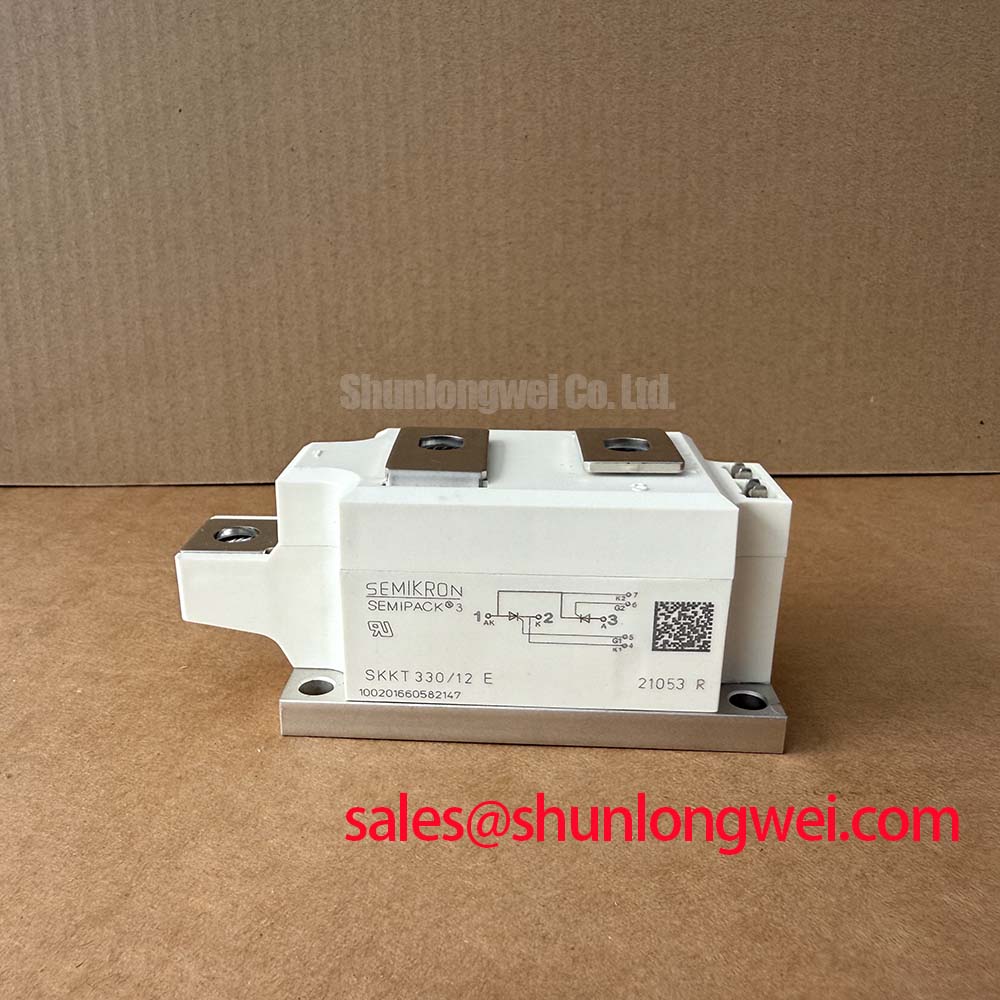
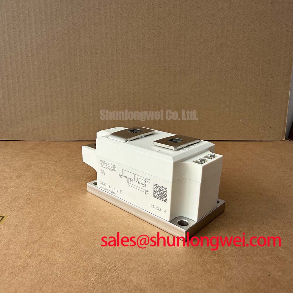
Before energizing a replacement position, verify the nameplate boundary of SKKT 330/12E, inspect the SEMIPACK 3 housing and terminals for handling damage, and confirm that the connected gate leads correspond to the equipment schematic.
The Semikron SKKT 330/12E is a dual thyristor module in the SEMIPACK 3 case format. Its official repetitive peak off state and reverse voltage ratings are VDRM and VRRM 1200 V. The official average on state current rating is ITAV 330 A at Tc 85°C, while the RMS current rating is ITRMS 510 A. These values define the module identity and should be checked against the original converter documentation before installation.
| Official Specification | Value | Condition or Scope |
|---|---|---|
| Repetitive peak off state voltage | 1200 V | VDRM |
| Repetitive peak reverse voltage | 1200 V | VRRM |
| Average on state current | 330 A | ITAV at Tc 85°C |
| RMS on state current | 510 A | ITRMS |
| Surge current | 9500 A | ITSM, 10 ms |
| Surge energy integral | 450,000 A²s | I²t |
| Maximum gate trigger voltage | 3 V | VGT |
| Minimum gate trigger current | 200 mA | IGT |
| Junction to case thermal resistance | 0.11 K/W | Per thyristor |
| Case style | SEMIPACK 3 | Mechanical package |
Field Diagnostics & Commissioning: Turn On Current Rise Limiting to Prevent Stress in SKKT 330/12E Topologies
Start commissioning with the power stage isolated from its normal command sequence. Check that each gate circuit reaches the intended thyristor gate terminal, that the return path has not been shared with a high current power connection, and that the polarity used by the original firing board is preserved. The stated VGT 3 V maximum and IGT 200 mA minimum under the applicable test conditions are official trigger characteristics, not a complete gate drive prescription. A firing circuit must be validated against the original equipment waveform and timing requirements.
In phase controlled capacitor switching or grid connected static var compensator equipment, unwanted turn on can arise when a steep commutation transient couples into a gate loop or appears across an off state device. RC snubbers, metal oxide varistors, and series saturable reactors are system level measures that can be evaluated for controlling transient voltage and current rise. Their component values, energy capability, and placement cannot be derived from the listed module ratings alone. The system engineer should capture voltage across the module, gate to cathode behavior, and current rise during the actual switching sequence before changing any suppression network.
The official 9500 A, 10 ms ITSM and 450,000 A²s I²t ratings are useful for fault coordination review, but they do not independently select a fuse. Compare the prospective fault waveform and the protective fuse clearing characteristic with the module I²t capability, considering the full branch impedance and the converter operating state. A fuse coordination decision requires the fuse manufacturer curve and the equipment fault study.
⚡ Safety Interlock Note: Isolate all stored energy sources and verify the capacitor bank is discharged before removing gate or power connections from the module.
Mechanical clamping and electrical connection quality directly affect repeatable current sharing between the two thyristors. Clean, flat mating surfaces, the specified fastening hardware, and torque values from the applicable equipment and package documentation should be used. Excessive fastening force can damage a module or terminal assembly, while insufficient force can raise contact resistance and create localized heating. The published SEMIPACK family context is available through Semikron SEMIPACK thyristor and diode module information.
Preventing Spurious Faults: Dynamic Firing Delay Angle Adjustment Under Guidelines for SKKT 330/12E
For an AC controlled rectifier or thyristor switched capacitor branch, firing angle changes the interval in which the thyristor conducts relative to the AC waveform. As the firing delay is moved away from the voltage crossing toward later portions of the half cycle, the transferred power and current waveform change, while displacement power factor and reactive power behavior can also change. The practical effect depends on the complete topology, source impedance, capacitor bank configuration, load conditions, and controller logic.
During field diagnosis, compare the firing commands for both thyristor sections with the relevant phase voltages using isolated measurement equipment. Inspect whether the expected pulse arrives on each intended half cycle, whether timing remains stable when the controller changes demand, and whether gate return paths remain quiet during high current commutation. A missing or displaced pulse may be related to the control board, isolation interface, timing reference, gate wiring, or the power circuit. It should not be assigned to the module from a single static measurement.
The 330 A ITAV rating at Tc 85°C must be considered alongside the actual conduction angle and measured case temperature. In a thyristor switched capacitor assembly, current can be discontinuous and strongly dependent on the connection point and network conditions. Designers should verify RMS current, repetitive voltage, commutation conditions, and thermal behavior under the equipment’s highest expected operating demand rather than treating the nominal current label as a system operating point.
Where an existing design uses a different member of the same product family, such as SKKT273/12E, electrical ratings, thermal paths, terminal arrangement, gate wiring, and protection coordination should be compared against the original assembly documentation. Similar family naming does not establish interchangeability. A replacement review should preserve the original topology and verify all relevant operating boundaries.
In systems that combine an upstream rectification section with a controlled thyristor branch, a module such as SKKD162/12 can appear elsewhere in the power chain as a diode module. Its function, terminal configuration, and protection requirements differ from those of the dual thyristor SKKT 330/12E. Treat each device according to its documented circuit role rather than by package resemblance.
Assembly Integrity & Layout Architecture: Preventing Localized Gate Hotspot Burnout for SKKT 330/12E
Inspect the gate trigger path as a complete loop from the firing transformer or isolated driver to the gate and cathode connections. Long parallel runs near high current busbars can pick up common mode noise during commutation. Design Consideration: keep the gate and cathode return path compact and paired where practical to reduce coupled disturbance, then verify the result with measurements taken during switching events.
The official gate trigger data establish that the module has a specified minimum trigger current of 200 mA under the applicable test conditions and a maximum trigger voltage specification of 3 V. They do not state a required pulse rise rate, holding current, latching current, pulse duration, negative gate bias requirement, or multipulse pattern. These values must be verified from the specific module documentation and the original control architecture. A thyristor is latched by anode current after successful triggering and is not turned off through a conventional gate turnoff command.
Where the original controller uses repeated firing pulses, the purpose is commonly to improve firing certainty across changing load and supply conditions. Any adjustment should be assessed by observing the real gate waveform and anode current response. Avoid assuming that a stronger pulse or a negative gate condition improves reliability without confirming the permitted limits for the device and driver. Gate circuit changes can alter noise susceptibility, trigger symmetry, and stress on the isolation components.
Power bus layout also influences the observed gate environment. Arrange forward and return current paths with low loop area where the assembly permits, especially around commutating branches and surge suppression components. This is an Engineering Recommendation rather than an official SKKT 330/12E specification. The desired result is reduced inductive overshoot and less coupled noise, verified against the module voltage rating during representative switching tests.
For broader context on power semiconductor application assessment, including industrial converter environments, consult Industrial Applications. The principles of measured voltage margin, controlled thermal paths, and documented protection coordination remain relevant, while final implementation must reflect the characteristics of this thyristor module and its host equipment.
SKKT 330/12E Operational Boundaries: Evaluating Reverse Recovery Charge Temperature Coefficient Limits
The SKKT 330/12E is identified here by its official dual thyristor ratings and does not include published diode reverse recovery values in the supplied specification set. No specific reverse recovery peak current, recovery time, recovery charge, softness factor, or temperature coefficient should be assigned to this model without the applicable manufacturer datasheet. Such figures are device specific and cannot be inferred from the 1200 V, 330 A, or SEMIPACK 3 identifiers.
In a commutated power stage, reverse recovery behavior may instead belong to an external diode, a separate diode module, or another branch in the system. When turnoff transients or radiated noise are observed, measure the involved device voltage and current paths with suitably rated instrumentation, then compare the waveform with the circuit diagram and known good operating data. Apparent overshoot can be influenced by busbar inductance, probe arrangement, suppression components, commutation current, and the timing of adjacent switching elements.
The 0.11 K/W junction to case thermal resistance per thyristor is an official thermal specification that supports thermal path evaluation. It does not define the complete thermal resistance to ambient because heatsink performance, interface condition, airflow, mounting pressure, and enclosure conditions belong to the equipment. When integrating the SKKT 330/12E, system engineers should measure case temperature and validate junction temperature margins under the actual duty cycle.
For module family and package level reference, the Semikron Danfoss power modules catalog provides product line information. Final maintenance decisions should remain tied to the original equipment schematic, documented protection network, measured electrical waveforms, and the official ratings listed for the installed module.