




Content last revised on October 1, 2026
SKM145GB128DN Thermal and Electrical Optimization
| Parameter | Official Specification |
|---|---|
| Manufacturer | Semikron |
| Model | SKM145GB128DN |
| Product category | IGBT Module |
| Rated voltage | 1200.0 V |
| Rated current | 145.0 A |
| Package | Semitrans |
With the DC link isolated, inspect the gate, emitter, and power-terminal connections for contamination, looseness, or visible heat damage before connecting an oscilloscope probe. A gate waveform that shows repeated ringing, a delayed turn-off edge, or an unexpected rise during the opposite device's switching interval requires measurement of the complete gate-drive loop, including the return path.
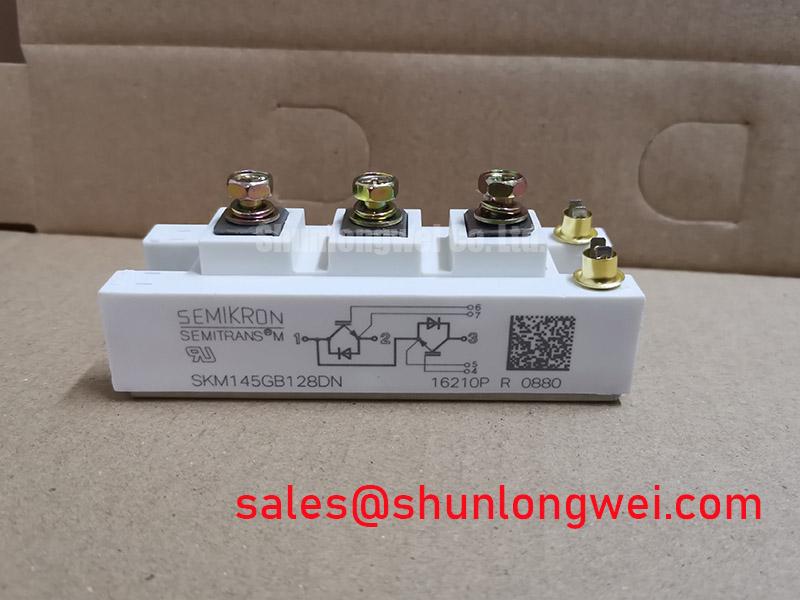
The SKM145GB128DN is a Semikron IGBT module with an official voltage rating of 1200.0 V and an official current rating of 145.0 A. These ratings identify the component's nameplate electrical class; they do not establish a complete system operating limit. Switching frequency, DC-link conditions, thermal impedance, pulse duration, gate-drive behavior, and converter protection settings must be evaluated at system level.
Active Miller clamp circuits can be considered when high dv/dt causes an unintended gate-voltage rise on the inactive IGBT. The clamp should use a low-inductance return path referenced to the appropriate emitter connection. Designers should verify the clamp's activation threshold, propagation delay, current capability, and behavior during short-circuit or desaturation protection events. The negative gate-bias range proposed for a particular converter is a system design choice, not an official specification established by the core parameters supplied for this product. Any negative bias, including values such as −5 V to −15 V, must be verified against the actual gate-emitter ratings and the manufacturer's complete device documentation.
Use a differential voltage probe or an isolated probing method suitable for the converter's common-mode voltage. Compare the gate-emitter waveform at the module terminals with the signal at the driver output. A large difference may indicate parasitic inductance, an unsuitable probe connection, driver return-current coupling, or an abnormal gate resistor network. The Precision Gate Drive Design reference provides a useful engineering context for reviewing this loop without treating a general gate-drive method as a model-specific guarantee.
For a commercial string inverter or micro-grid energy-storage converter, the system integrator should verify dead time, interlock behavior, gate-drive isolation, short-circuit response, and peak VCE during switching tests. The Semikron-Danfoss SEMITRANS industry information can provide broader package and product-family context, while the exact application limits remain dependent on the applicable technical documentation and converter design.
Benchtop Waveform Tuning and Auxiliary Emitter Return Separation
Probe the auxiliary emitter return and the main power-emitter return separately during a controlled switching test; a visible voltage difference between those paths is evidence that common-emitter coupling must be investigated before changing gate-drive values.
When the driver return shares a high-current emitter trace, the voltage developed by the switching current can appear as false feedback at the gate driver. This may produce oscillation, uneven turn-off, or apparent Miller turn-on. The preferred layout principle is to keep the driver return path associated with the intended auxiliary emitter connection and to prevent high-current commutation paths from flowing through that measurement reference. The final copper geometry, clearance, and connection method should be determined from the module terminal arrangement and the complete power-loop layout.
Benchtop tuning should begin with low-energy switching and a known-good measurement setup. Record gate-emitter voltage, collector-emitter voltage, collector current, and heat-sink temperature together so that electrical overshoot is not evaluated separately from thermal stress. If the waveform changes when the probe ground or cable position changes, treat the result as a measurement-loop issue until the signal is reproduced with an appropriate differential method.
The requested 2 kHz to 16 kHz switching range should be treated as an evaluation range rather than a guaranteed operating window for this module. Increasing switching frequency generally raises switching losses and reduces the time available for heat removal, but the resulting junction temperature depends on load current, modulation, pulse pattern, mounting quality, heat-sink performance, and ambient conditions. Designers should calculate losses from the applicable switching and conduction data, then verify the result with temperature measurements under the intended duty cycle.
For equipment exposed to dust, condensation, or fluctuating ambient temperature, inspect the heat-sink fins, fan path, interface material, and terminal condition during scheduled maintenance. Maintenance Note: Record contact-temperature trends and clean the cooling path before thermal drift becomes an intermittent shutdown.
In a converter with a separate rectifier or auxiliary power stage, the SEMIX403GB128DS may be reviewed as a related component reference for topology coordination. It should not be treated as an automatic replacement or a guaranteed companion device for the SKM145GB128DN.
Circuit Protection and Reliability Evaluation
When a converter trips during a high-energy switching event, capture the DC-link voltage, collector-emitter voltage, gate-emitter voltage, and protection timing on the same trigger rather than assigning the failure to one waveform alone.
Desaturation protection, soft turn-off, gate interlock, and short-circuit response are system-level protection functions. The supplied official parameters confirm the 1200.0 V voltage class and 145.0 A current class, but they do not provide a short-circuit withstand time, soft-shutdown profile, FIT rate, or Single Event Burnout probability. Those values must not be inferred from the part number or nameplate ratings.
Terrestrial neutron exposure and altitude-related reliability may be relevant in installations above 2000 m, but a defensible FIT calculation requires a defined radiation model, device technology data, operating-voltage distribution, mission profile, and validated failure-rate methodology. Without those sources, the correct engineering action is to evaluate DC-link headroom, switching overshoot, insulation coordination, cooling, and protection timing through qualification testing. Do not convert altitude alone into a numerical SEB rate or a guaranteed lifetime prediction.
During fault analysis, inspect whether the protection circuit detects the event quickly enough to limit energy and whether the gate driver maintains the intended turn-off behavior under high common-mode transients. Check the current sensor, desaturation blanking, clamp path, driver supply, and gate-emitter return as a complete chain. A failed module may reflect electrical overstress, inadequate cooling, an abnormal load, or a protection interaction; the physical evidence and captured waveforms should determine the next test.
For parallel IGBT operation, positive temperature coefficient behavior can assist static current sharing, but it does not guarantee equal dynamic current distribution. Differences in gate-loop impedance, emitter inductance, propagation delay, thermal coupling, and commutation layout must be measured. Any multi-module arrangement should be validated with current probes and thermal measurements across the intended operating envelope.
Assembly Integrity and Transient Thermal Architecture
Measure the temperature rise at the module case and heat-sink interface after a controlled load cycle, then inspect the interface for pump-out, voiding, contamination, or uneven pressure before attributing a thermal fault to the semiconductor.
The Semitrans package provides the mechanical interface for mounting and cooling, while the actual transient thermal response depends on the module construction, interface material, heat sink, cooling method, pulse profile, and mounting condition. A transient thermal model can use a junction-to-case RC network when the required thermal impedance data is available from the applicable manufacturer documentation. The model should be checked against measured case and heat-sink temperatures rather than used as a substitute for validation.
For a pulsed overload, calculate the expected junction-temperature rise from the time-dependent power loss and the relevant transient thermal impedance curve. The resulting peak must be compared with the permitted junction-temperature limit from the complete technical documentation. The supplied 1200.0 V and 145.0 A values are electrical ratings; they do not define a permissible overload duration or a thermal recovery window.
Inspect the mounting plane for flatness and confirm that the heat-transfer interface is continuous across the active module base. Apply the selected interface material according to its technical data, maintain even fastener loading, and verify that power-terminal tightening does not distort the module or transfer mechanical stress into the base. The appropriate torque is determined by the manufacturer's mechanical instructions and the selected hardware, not by the voltage or current rating.
In commercial string inverters and micro-grid storage systems, review the entire thermal path during service: airflow direction, filter loading, fan control, enclosure condensation, heat-sink fouling, and cable termination temperature. When comparing possible devices for a repair or redesign, the SEMIX302GB126V1 comparison material may support a neutral parameter review, but electrical, mechanical, gate-drive, and thermal compatibility must still be demonstrated in the target converter.