Content last revised on October 5, 2026
SKM150GB128D Operational Boundaries: Managing High-C-Rate Battery Cycling
In a commercial string inverter or micro-grid energy-storage converter, the module may be evaluated in the power path between a battery rack, a DC link, and a bidirectional inverter bridge. During charging, stored energy moves from the AC conversion stage toward the battery. During discharge or peak shaving, the direction reverses. The semiconductor therefore experiences switching conditions that depend on DC-link voltage, load current, modulation strategy, switching frequency, cooling performance, and the control system’s current-limiting response.
The 1200.0 V voltage rating and 150.0 A current rating are official device values, not a complete operating envelope for every battery-cycling condition. System designers should verify the actual DC-link range, transient overshoot, repetitive current profile, short-circuit protection response, junction-temperature calculation, and fault-clearing sequence against the relevant Semikron documentation. Battery charge and discharge current can change rapidly during peak shaving, so the complete commutation path must be checked rather than judging suitability from the nameplate current alone.
For a replacement assessment, isolate the converter, discharge the DC link according to the equipment service procedure, and record the original gate-drive connections before removing the failed part. Inspect adjacent busbars, snubber components, gate resistors, driver outputs, and current sensors. A failed IGBT may be a consequence of an upstream gate-drive or commutation problem, so fitting a replacement without checking those circuits can produce a repeat failure.
When comparing related Semikron parts, the SKM75GB07E3 can be reviewed as a separate reference device, but its voltage, current, internal circuit arrangement, terminal layout, and thermal capability must be checked independently. It should not be treated as an automatic substitute for the SKM150GB128D.
Benchtop Waveform Tuning: Optimizing Heatsink Contact Pressure and Gate Drive on the SKM150GB128D
Thermal installation is the first bench check after electrical compatibility. Clean the heatsink and module mounting surface, inspect both surfaces for burrs or visible curvature, and apply the approved thermal interface material as a uniform thin layer. The supplied project requirement identifies a 50 to 100 micrometre interface target as a general integration consideration, not as an official SKM150GB128D factory specification. The final interface method should follow the module documentation and the thermal compound supplier’s instructions.
Mounting pressure should be introduced progressively and symmetrically so that the baseplate is not pulled unevenly against the heatsink. Designers should verify the correct screw sequence, fastener type, washer arrangement, and torque from the applicable Semikron mechanical documentation. Excess compound, trapped air, contamination, or uneven pressure can increase thermal resistance and create local temperature differences during high-current cycling.
Field Alert: Disconnect the DC link and gate-drive supply before removing any terminal or probing a gate circuit, and follow the equipment’s verified discharge procedure.
Gate-drive commissioning should begin with low-risk bench measurements. Confirm that the driver can source and sink the required gate current for the selected switching speed, while checking the driver’s isolation, supply stability, undervoltage behavior, and protection timing. The external gate resistor is a tuning component rather than a universal fixed value. Increasing damping can reduce ringing but may increase switching loss; reducing it can accelerate transitions while increasing sensitivity to layout inductance, driver impedance, and device variation.
Use a suitable differential probe and a short, controlled measurement connection when examining gate-emitter and collector-emitter waveforms. Look for abnormal ringing, delayed turn-off, unequal switching between parallel paths, or a gate signal that changes when the power stage is loaded. These observations may indicate a driver, layout, probe, or commutation issue. Compare the signal with a known-good channel and confirm the result under the intended operating conditions.
SKM150GB128D Operational Boundaries: Evaluating PCB Symmetry Considerations for Dual IGBT Limits
A dual-IGBT module requires careful separation of high-current power paths and low-noise gate-drive returns. The main emitter current path carries substantial switching current and can develop voltage changes across its stray inductance. The auxiliary emitter or driver return, where provided by the actual module configuration, should be routed according to the manufacturer’s terminal definition and kept separate from the high-current return until the intended reference point.
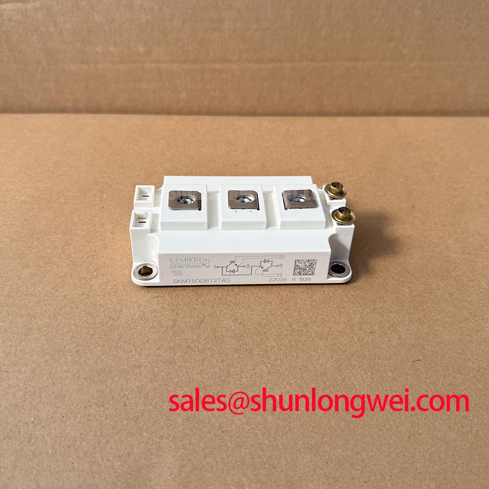
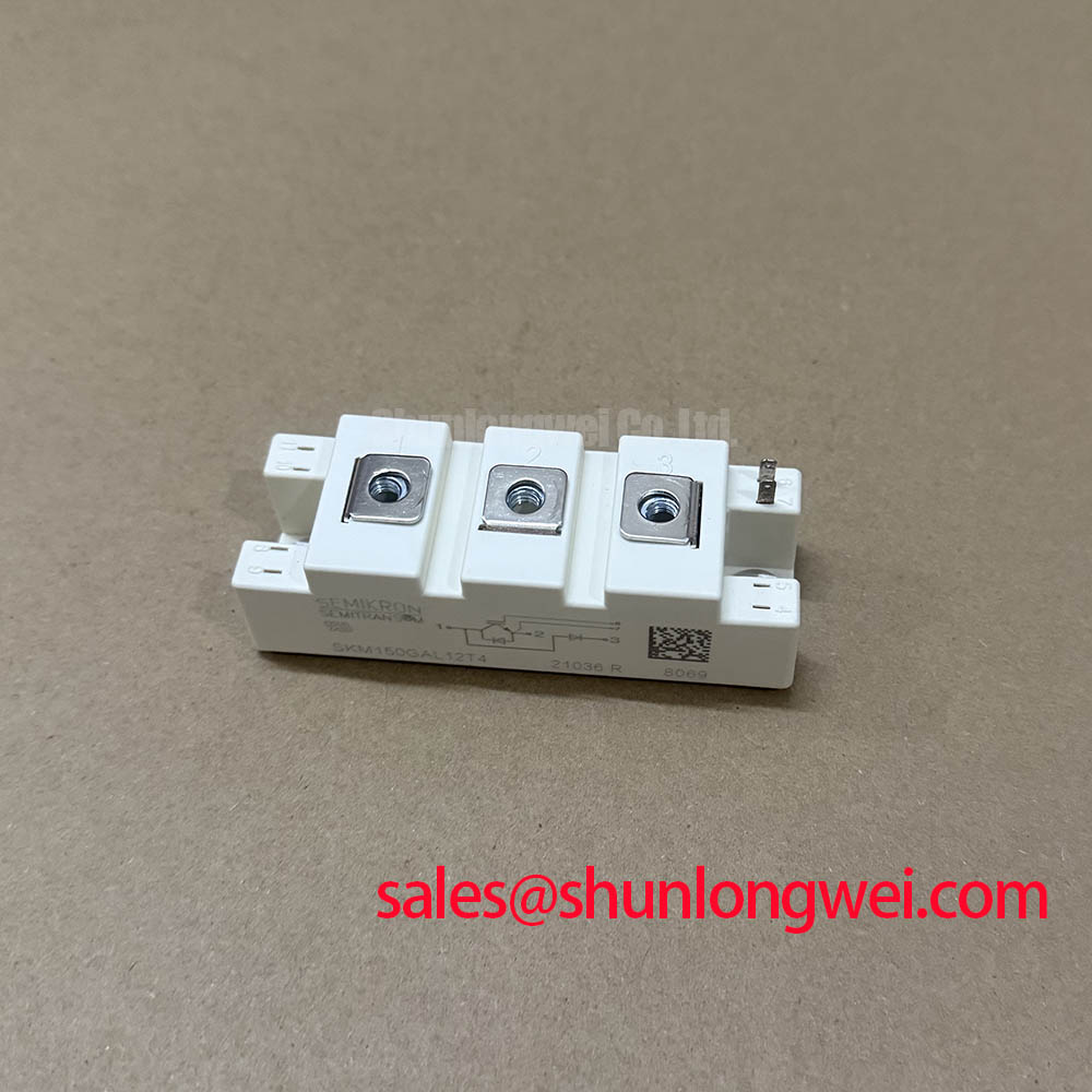
This is a Design Consideration, not a confirmation of an internal terminal arrangement beyond the supplied product data. The system integrator should verify the exact pinout and circuit topology from the original Semikron drawing before laying out a replacement board. Do not infer terminal functions from a visually similar Semitrans package or from another part number.
Keep the two switching channels geometrically balanced where the circuit uses paired IGBTs. Match the gate-loop path, avoid unnecessary vias in the driver return, and prevent the power emitter trace from sharing a narrow section of copper with the control reference. The objective is to reduce mutual coupling and maintain a stable gate reference during fast current changes. Final spacing, creepage, clearance, copper thickness, and insulation coordination remain system-level decisions governed by working voltage, pollution environment, altitude, transient category, and applicable safety requirements.
During troubleshooting, measure the gate-emitter waveform at the module terminals rather than at the driver output alone. If a channel appears to switch correctly on the bench but behaves differently under load, inspect the complete return path, gate resistor connection, driver isolation, terminal pressure, and busbar symmetry. A waveform difference may indicate impedance imbalance, parasitic coupling, or an instrument connection problem; verify it against the known-good channel with the same probe method.
In a larger conversion chain, an upstream rectifier or complementary power stage may be reviewed alongside the inverter bridge. The SKM100GB063D is presented as a separate reference product for topology evaluation, not as a prescribed replacement. Its ratings and circuit configuration must be confirmed independently before use in the same system.
Assembly Integrity & Layout Architecture: Implementing High-Frequency Commutation Loop Inductance for SKM150GB128D
Switching overshoot is governed by the interaction between stray commutation inductance, current slew rate, device behavior, busbar geometry, and the DC-link capacitor position. In engineering analysis, the peak collector-emitter stress is commonly considered as the DC-link voltage plus the inductive contribution produced by the switching current change. This relationship is useful for interpreting oscilloscope results, but it does not establish a universal clamp voltage, switching speed, or inductance limit for the SKM150GB128D.
The practical objective is to minimize the high-frequency commutation loop area. Place the high-frequency DC-link capacitor close to the module power terminals, keep the outgoing and return conductors adjacent, and use a symmetrical planar busbar arrangement where the mechanical design permits it. The design team must calculate the resulting parasitic inductance and verify peak voltage against the module’s documented switching limits under the real DC-link and load conditions. The supplied 25 nH value should not be treated as a factory requirement for this product.
Snubber selection also belongs to the complete converter design. A capacitor that is too small may provide limited suppression, while excessive capacitance can increase switching loss and circulating current. Select and validate the snubber using measured ringing frequency, voltage stress, pulse energy, capacitor impulse capability, resistor loss, and the available mechanical connection. Confirm the result with a properly rated differential probe and a controlled load test.
Before energizing a repaired inverter, inspect busbar insulation, terminal flatness, mounting pressure, gate-driver connectors, and the condition of nearby capacitors and resistors. Check for unintended continuity between control and power returns, then perform a low-energy functional test with current limiting where the equipment permits it. Record the switching waveform at the module terminals and compare both directions of power flow, since a converter that behaves acceptably while charging can show a different commutation profile during battery discharge.
For broader procedures covering component testing and failure analysis, consult the Field Engineer’s Handbook. The Semitrans product family can also be reviewed through the Semikron-Danfoss SEMITRANS® Industry Standard IGBTs product information. Final approval remains dependent on the applicable data sheet, converter test results, thermal design, protection circuit, and equipment safety evaluation.