
Content last revised on October 27, 2026
SKM400GAL12T4 Module Overview and Pre-Energization Checks
- Measure cold-state resistance across the main terminals and compare the reading with a known-good assembly before energizing the converter.
- Check the insulated copper baseplate interface, heatsink flatness, thermal compound coverage, and mechanical seating.
- Inspect gate-driver isolation, connector polarity, gate-emitter connections, and the complete low-inductance drive return path.
- Confirm the DC-link voltage class, braking resistor arrangement, switching sequence, and protection coordination against the equipment schematic.
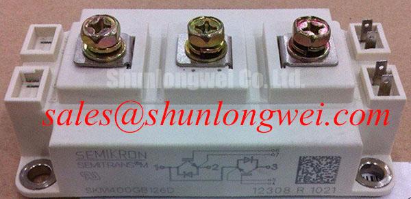
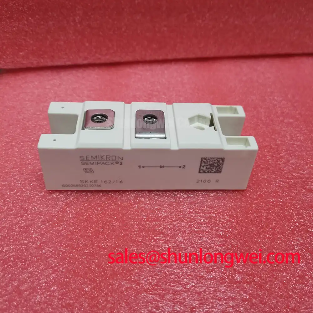
SKM400GAL12T4 is a Semikron SEMITRANS 3 IGBT module using the GAL boost-chopper topology. Its published electrical ratings make it relevant to high-power braking choppers and single-switch boost stages, including traction inverter DC-link braking circuits subject to complete system-level validation.
| Parameter | Specification or Application Reference | Engineering Relevance |
|---|---|---|
| Collector-emitter voltage | VCES = 1200 V | Supports evaluation in 400 V to 800 V DC bus topologies, with switching overshoot assessed at system level. |
| Continuous collector current | IC = 400 A at Tc = 80 °C | Provides a high-current operating reference for industrial power conversion equipment. |
| Collector-emitter saturation voltage | VCE(sat) = 1.80 V typical at Tj = 125 °C, subject to the datasheet current and gate-voltage test conditions | Supports conduction-loss estimation using the actual duty cycle, current waveform, and junction temperature. |
| Junction-to-case thermal resistance | Rth(j-c) = 0.075 K/W | Defines the IGBT junction-to-case thermal path used in the heatsink calculation. |
| Circuit topology | GAL boost chopper | Matches single-switch boost and braking-chopper circuit arrangements, subject to terminal and diode orientation checks. |
| Switching frequency | Application-dependent; 20 kHz must not be treated as a guaranteed maximum operating frequency | Requires switching-loss and thermal verification at the intended operating conditions. |
| Package | SEMITRANS 3 | Provides a mechanically robust industrial module format for bolted heatsink installation. |
The positive temperature coefficient of saturation voltage in the relevant operating region can assist static current sharing when multiple devices are evaluated in parallel, but dynamic sharing remains dependent on gate-loop symmetry, commutation layout, device tolerances, and driver timing. The original equipment circuit must therefore be compared terminal by terminal before replacement.
Preventing Spurious Faults: Braking Resistor and Chopper Guidelines for SKM400GAL12T4
The braking resistor and chopper switch must be assessed as one energy-management path rather than as isolated parts. During motor deceleration, regenerative energy raises the DC-link voltage; the chopper then directs this energy into the ballast resistor. Resistor pulse energy, peak power, thermal recovery, duty cycle, and the chopper conduction interval should be calculated from the actual vehicle or machine deceleration profile. The 1200 V VCES rating is an official device limit, not a substitute for measuring the peak voltage generated by wiring inductance and switching transients.
For a traction inverter, the braking branch should be checked against the maximum DC-link operating condition, the resistor’s short-duration overload capability, and the available fault-clearing path. Gate-driver protection must respond within the module’s specified short-circuit withstand conditions; a semiconductor fast fuse or equivalent protective device must also be coordinated with the installation’s available fault energy and must not be assumed to protect the IGBT by itself. An I2t comparison is useful only when the fuse curve, bus capacitance, loop inductance, gate-driver response, and prospective fault current are known together.
Layout has a direct effect on nuisance overvoltage trips. Keep the high-current DC-link and braking loop compact, use a symmetrical laminated bus structure where practical, and avoid routing the gate-drive return beside the high-di/dt collector path. Clearance and creepage must follow the insulation system used by the equipment, contamination level, and working-voltage requirement; the package rating alone does not establish the complete cabinet insulation design.
When commissioning a replacement, record the DC-link voltage during acceleration release, emergency braking, and repeated braking events. A fault that appears only during repeated deceleration may involve resistor thermal accumulation, control timing, or bus-voltage regulation rather than an immediate semiconductor defect. The Field Engineer’s Handbook can be used as a practical reference for structured testing and failure analysis.
For a topology comparison, engineers may also evaluate the SKM400GAR124D as a related Semikron device, while checking its topology, ratings, terminal arrangement, and thermal data independently rather than assuming interchangeability.
SKM400GAL12T4 Circuit Protection & Reliability: Damping Commutation Oscillations
Reverse-recovery behavior in the commutation path can create a transient current peak, ringing, and additional voltage stress when the braking switch turns on. This is distinct from the IGBT tail current that occurs during turn-off. The peak reverse-recovery current and the rate of current change depend on the companion diode, DC-link inductance, busbar geometry, junction temperature, load current, and gate-driver impedance. These values must be captured with a suitable current probe and differential voltage probe during controlled switching tests.
An RC snubber may reduce high-frequency ringing, but its capacitance, resistance, pulse energy, and physical placement are system-design variables. Install the snubber loop close to the switching-current path, then verify that the added capacitive current does not create unacceptable turn-on loss. A resistor inserted in the gate path can also shape the switching edge, although the final value should be selected from measured gate voltage, collector-emitter voltage, current, and temperature behavior.
Desaturation protection should detect abnormal on-state collector-emitter voltage quickly enough to limit fault energy while avoiding false trips during normal switching transients. The commonly discussed sub-microsecond or few-microsecond protection region is a design objective, not an official SKM400GAL12T4 rating. The actual response must include blanking behavior, diode charging, driver propagation delay, cable length, and the selected soft turn-off sequence.
A two-stage soft turn-off strategy can reduce the voltage excursion associated with abruptly removing gate charge. The first stage limits the fault current transition, while the final stage establishes the off-state condition. Engineers should verify the complete sequence with the driver manufacturer’s timing data and an appropriately rated isolated or differential oscilloscope measurement at the module gate terminals. A protection board that works on a low-inductance laboratory fixture may behave differently in a traction cabinet because the commutation loop and gate loop are physically larger.
💡 Pro Tip: Keep the power commutation loop and gate-driver return physically separated, then validate the resulting overshoot and gate oscillation with a double-pulse or equivalent controlled switching test before full-load operation.
The Semikron discussion of single-sided sintering technology provides useful background on thermal packaging concepts, but it should not be used to infer unlisted electrical or mechanical limits for this specific module.
SKM400GAL12T4 Operational Boundaries: Preventing Terminal Overheating
Terminal heating is often governed by contact resistance, current distribution, joint pressure, conductor geometry, and local airflow. A high-current module can show acceptable semiconductor temperature while a loose, contaminated, or unevenly clamped bolted connection develops a localized hot spot. Measure the complete joint with a calibrated micro-ohmmeter after the equipment is isolated and the DC link is safely discharged, and compare corresponding terminals under the same test conditions.
A contact-resistance reference of less than 10 µΩ should be treated as a system inspection target only when it is defined by the equipment manufacturer and measured with a suitable four-wire method. It should not be treated as an SKM400GAL12T4 specification. Probe placement, cable force, surface condition, and parallel current paths can materially change the reading.
Thermographic inspection should be performed after the converter reaches a representative load condition and during the longest expected braking or boost interval. Compare the temperature profile around each power terminal, the busbar interface, the heatsink, and adjacent insulation. A gradual rise across the entire assembly suggests a different thermal condition from a concentrated hot spot at one fastener, but the image must be interpreted alongside load current and ambient temperature.
The Rth(j-c) = 0.075 K/W value applies to the IGBT junction-to-case thermal path. It does not include thermal interface material, heatsink resistance, mounting pressure, airflow, or enclosure effects. When fitting the SEMITRANS 3 housing, clean mating surfaces, maintain even mechanical pressure, and use the thermal interface method specified by the equipment build documentation. No package material or internal construction should be assumed beyond published information. General background on PPS engineering plastic is available from Polyphenylene sulfide references.
Operating interval limits should be derived from the actual current waveform and thermal recovery between pulses. A continuous-current inspection based only on the nominal 400 A at Tc = 80 °C rating does not represent every pulse pattern. For high-speed rail and heavy freight locomotive traction inverters, engineers should correlate terminal thermography with braking frequency, enclosure airflow, busbar temperature, and the heatsink thermal time constant before approving a replacement assembly.
SKM400GAL12T4 Operational Boundaries: Suppressing Cres-Induced Gate Voltage Spikes
High dv/dt at the switching node can couple through the reverse transfer capacitance, often represented in the switching model by Cres, and raise the gate voltage of an off-state IGBT. If the induced gate voltage reaches the IGBT’s turn-on region, unintended conduction becomes possible; in circuits with complementary active switches, this may cause cross-conduction. The correct countermeasure begins with a low-inductance gate loop, a short gate-emitter return, and a driver architecture capable of actively holding the inactive gate in the off state.
An active Miller clamp can provide a low-impedance path during the high-voltage transition. Its effectiveness depends on the clamp threshold, propagation delay, driver source and sink capability, gate resistance, and the voltage measured directly at the module terminals. A negative gate bias may be considered by the system designer, but the frequently cited range of −5 V to −15 V is not an official SKM400GAL12T4 requirement and must not be applied without checking the driver and module gate-emitter limits.
Use separate power and signal references where the driver architecture requires them, and avoid sharing a narrow return trace with the emitter-current path. The gate waveform should be observed during the fastest relevant switching-node transition, not only during a slow bench turn-on. Look for positive gate spikes, negative undershoot, ringing near the Miller plateau, and timing differences between paralleled branches.
When several modules or switching devices operate in parallel, positive temperature coefficient behavior in the relevant operating region may support static current balance, while dynamic balance still depends on matched gate impedances and symmetrical busbar geometry. The current-sharing assessment should include the highest expected temperature, the shortest switching interval, and the worst practical tolerance combination. Any active clamp or two-level turn-off setting should be validated against the measured collector-emitter overshoot and driver dissipation before the traction inverter is returned to service.