

Content last revised on September 28, 2026
FS400R12A2T41 Ratings and Commissioning Context
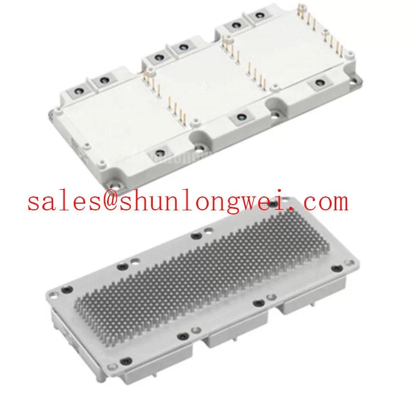
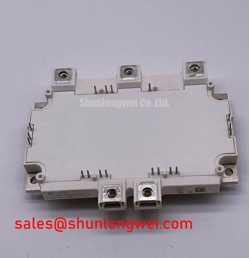
Begin commissioning by isolating the DC link, checking the module identification against the service record, and measuring the power-terminal condition before applying control power. The Infineon FS400R12A2T41 is a 1200 V, 400 A half-bridge IGBT module in the EconoDUAL™ 3 package. Its continuous collector-current rating is specified at 400 A with Tc = 80°C, while the typical collector-emitter saturation voltage is 1.85 V at Ic = 400 A and Tvj = 125°C. The maximum junction temperature is 175°C.
These values identify the electrical boundary of the device, but they do not by themselves establish the allowable current, switching frequency, overload duration, or thermal margin of a complete traction inverter. When evaluating a replacement in a high-speed rail or heavy freight locomotive traction inverter, the system engineer should verify the original gate-driver interface, DC-link topology, cooling arrangement, protection thresholds, and switching test results.
| Parameter | Official Specification |
|---|---|
| Manufacturer | Infineon |
| Part number | FS400R12A2T41 |
| Collector-emitter voltage | 1200 V VCES |
| Continuous collector current | 400 A at Tc = 80°C |
| Typical collector-emitter saturation voltage | 1.85 V at Ic = 400 A, Tvj = 125°C |
| Maximum junction temperature | 175°C |
| Package | EconoDUAL™ 3 |
| Internal configuration | Half-bridge |
Field Diagnostics and Commissioning for Impedance Mismatch in FS400R12A2T41 Topologies
During a field inspection, compare the DC-link voltage, phase-leg voltage, gate-emitter waveform, and motor-terminal waveform with a known-good converter or the approved commissioning record. A long motor cable can behave as a distributed transmission path rather than an ideal connection. Reflections may appear at cable and motor terminations, producing voltage ringing that is not visible at the inverter terminals. The observed stress depends on cable length, cable construction, motor impedance, switching speed, termination conditions, and the complete converter layout.
This is a Design Consideration, not an FS400R12A2T41 production guarantee: an apparent terminal spike approaching twice the local DC-link voltage can occur in some long-cable arrangements when reflected waves reinforce the incident edge. The correct response is measurement rather than a fixed filter value. Use a properly rated differential probe at the module terminals and at the motor end, confirm probe loop geometry, and correlate the waveform with gate timing and current commutation.
Output filters, common-mode chokes, and dv/dt limiting networks should be selected from the measured cable and motor behavior. Designers should verify semiconductor peak-voltage margins against the actual DC-link voltage during switching tests. Filter placement also matters. A network installed at the inverter output may reduce terminal stress, while a motor-end network can address reflected-wave behavior more directly. The traction system designer must determine the required topology, insulation coordination, cooling, and transient rating from the complete equipment architecture.
When checking a suspected impedance mismatch, inspect the phase conductors, shield termination, motor junction box, and return-current path before changing gate resistance. An abnormal waveform may also be associated with probe placement, unequal commutation paths, a loose laminated-bus connection, or a degraded snubber connection. Capture the same time base and voltage scale on all phases so that asymmetry can be separated from normal switching behavior.
The half-bridge configuration is relevant to regenerative braking. During braking, a chopper and braking resistor, where fitted, can absorb excess DC-link energy according to the vehicle control strategy and DC-link protection scheme. The FS400R12A2T41 rating does not define the braking resistor value, duty cycle, or allowable regenerative energy. Those values must be established from the traction inverter control system, resistor thermal model, DC-link capacitance, and measured duty profile.
For a neutral comparison during procurement or repair planning, engineers may review the FS100R12N2T4 alongside this 400 A half-bridge device. Any interchange assessment should confirm electrical ratings, mechanical fit, terminal arrangement, gate-drive requirements, thermal interface, and protection coordination rather than relying on current rating alone.
Preventing Spurious Faults Through Heatsink Contact Pressure and Switching Control
Remove contamination from the heatsink mounting surface and inspect the mating plane before installing the module. The EconoDUAL™ 3 package requires a mechanically stable thermal path. A bowed heatsink, uneven fastener loading, excessive thermal-interface material, or trapped air can increase thermal resistance and create local temperature differences between the upper and lower switching positions.
The following is a Design Consideration for general power-module assembly, not an official FS400R12A2T41 mounting specification: apply only the thermal-interface material required by the approved mechanical process, maintain consistent coverage, and tighten fasteners in the specified sequence using a calibrated tool. The exact material, thickness, screw sequence, and torque must come from the module mechanical documentation and the equipment manufacturer’s assembly procedure. Do not substitute a generic torque value for the approved installation data.
After installation, inspect the contact pattern where the procedure permits, then monitor temperature rise under a controlled load. A sudden phase-to-phase thermal difference may warrant checking heatsink flatness, interface coverage, terminal clamping, airflow, and current sharing. It should not be assigned to one cause without waveform and thermal evidence.
The freewheeling diode path also influences switching behavior. Reverse-recovery current can interact with stray inductance and the opposing IGBT, creating voltage overshoot, ringing, and electromagnetic interference. A snubber or dv/dt network can reduce the severity of this interaction, but its capacitance, damping, pulse-current capability, and physical placement are system design variables. Verify the result with a differential voltage probe and a current measurement method suitable for the converter’s pulse environment.
Gate-driver commissioning should include a check of the driver supply during repetitive switching. A bootstrap arrangement, where used by the original design, must maintain adequate high-side driver supply during the required pulse pattern. The designer should assess capacitor charging current, leakage, duty-cycle limitations, diode reverse recovery, undervoltage-lockout behavior, and the worst-case high-side on-time. The FS400R12A2T41 product data supplied here does not specify a bootstrap capacitor or diode, so those components must be verified from the gate-driver documentation.
For locomotive equipment that may experience low temperatures, condensation, or rapid thermal transitions, inspect conformal protection, enclosure sealing, connector condition, and the heatsink drainage path according to the vehicle maintenance procedure. Maintenance Note: Monitor contact-area temperature rise during scheduled service and recheck the cooling-air path after cleaning, because a visually clean heatsink can still have restricted internal airflow.
The Infineon EconoDUAL™ 3 product family information provides useful package-level context, but the final installation method remains dependent on the approved module and converter documentation.
Benchtop Waveform Tuning for High-Frequency Commutation Loop Inductance
Use a low-inductance test arrangement when examining the FS400R12A2T41 on the bench. The DC-link capacitor, module terminals, commutation path, snubber, and current sensor should be arranged so that the measured loop represents the final converter geometry. Long oscilloscope ground leads and remote probe connections can add ringing that is not present in the power stage, or conceal ringing that is present.
The physical relationship is straightforward: turn-off voltage rise increases with commutation current slope and stray inductance. In engineering terms, the inductive contribution can be viewed as the product of loop inductance and di/dt, added to the local DC-link voltage. This calculation is useful for identifying which layout change matters, but it is not a substitute for measuring the assembled converter. The system engineer must verify peak voltage, ringing frequency, damping, and repetitive stress at the intended temperature and load.
Keep the high-frequency commutation path compact and symmetrical. The positive and negative DC-link conductors should follow the approved laminated busbar or planar arrangement, with the snubber connected across the shortest practical electrical path. Clearance and creepage must be checked against the equipment insulation system, pollution environment, working voltage, and applicable railway or industrial standard. A low-inductance layout cannot compensate for inadequate insulation spacing.
Snubber selection should begin with the measured overshoot and ringing energy. A capacitor that is too small may have little effect; a capacitor that is too large can increase switching loss and capacitor pulse current. The resistor must be evaluated for pulse energy and temperature, while the capacitor voltage rating must cover the measured transient with the system’s required margin. These are Engineering Recommendations for bench tuning, not fixed values for this module.
When a waveform shows a high-frequency burst after diode commutation, compare the upper and lower switch positions and repeat the test with the snubber temporarily characterized through a safe, approved laboratory method. Check the DC-link capacitor connection, emitter and collector terminal clamping, busbar symmetry, and current-probe orientation. A difference between two nominally identical phase legs can point toward layout asymmetry, connection inductance, driver timing, or measurement error.
Thermal results must be interpreted with the switching waveform. The official typical saturation voltage of 1.85 V at 400 A and Tvj = 125°C is a specified reference condition, not a universal operating value. Actual conduction and switching losses depend on current, junction temperature, gate resistance, commutation conditions, diode behavior, and control timing. Designers should calculate losses from the relevant device curves and then confirm the result through temperature measurement.
Positive temperature behavior can assist static current sharing when multiple devices are used in a properly designed arrangement, but dynamic sharing remains affected by gate-loop inductance, driver matching, busbar geometry, thermal coupling, and switching timing. Parallel operation should therefore be validated with simultaneous current and voltage measurements rather than inferred from the nominal current rating.
For broader guidance on selecting switching devices, controlling parasitic effects, and assessing converter reliability, consult the Power Electronics Masterclass as an engineering reference. It should complement, not replace, the Infineon data applicable to the FS400R12A2T41.
Dynamic Gate Impedance Control for Robust FS400R12A2T41 Switching
Begin gate-drive tuning by measuring gate-emitter voltage at the module terminals, not only at the driver board. The measurement should include turn-on, turn-off, dead time, collector-emitter voltage transition, and the behavior of the inactive switch during the opposite device’s commutation. High dv/dt can couple through parasitic capacitances and produce an unintended gate excursion, but the observed result depends on driver impedance, gate-loop layout, common-emitter path, busbar coupling, and load current.
A dedicated Miller clamp can reduce the impedance presented to the gate during the high-voltage transition. Its activation timing, sink-current capability, isolation arrangement, and interaction with the gate resistor must be verified against the selected driver. An active clamp is not automatically suitable for every gate-driver topology, and its behavior must be checked during both hard switching and diode recovery.
Negative gate bias is sometimes used to increase turn-off immunity, but the permitted gate-emitter voltage range and driver supply arrangement must be confirmed from the official FS400R12A2T41 documentation and the selected gate-driver data. The supplied product parameters do not authorize a universal negative-bias value. The integrator should verify transient gate voltage, insulation coordination, driver undervoltage behavior, and turn-off energy before adopting any negative-bias scheme.
When a suspected cross-conduction event occurs, first confirm the timing relationship between both gate signals and the phase-leg voltage. Then inspect driver supply droop, isolation-barrier behavior, gate-loop return inductance, Miller-clamp timing, and the common-mode current path. A fault indication may also originate from desaturation protection, current-sensor saturation, DC-link disturbance, or control timing rather than from the IGBT itself.
Bootstrap high-side drivers require additional attention during low-frequency operation, pulse skipping, regenerative braking, and startup. The bootstrap capacitor must retain sufficient charge for the complete high-side gate-drive demand, while its diode and resistor path must recover charge within the available low-side interval. Engineers should verify this under the actual duty pattern, temperature range, leakage conditions, and driver quiescent current. If the traction inverter uses an isolated supply instead, the isolation supply’s transient response and common-mode capacitance become the relevant checks.
Shielding and grounding should be treated as a current-path problem. Keep power switching returns separate from sensitive control returns until the intended reference point, minimize gate-loop area, and route high-current commutation paths away from encoder, resolver, and protection wiring. The final arrangement should be validated with conducted and radiated measurements at system level; a semiconductor module cannot independently claim compliance with complete-equipment EMC requirements.
The Infineon OptiMOS™ Low Voltage MOSFETs information is relevant only when a separate low-voltage switching stage is being assessed; it does not establish interchangeability with this 1200 V IGBT half-bridge module.