Content last revised on October 5, 2026
VI-252-EV Operational Boundaries: Evaluating Negative Gate Bias and Active Miller Clamp Limits
Probe the external gate-driver output and the power-stage switching node with isolated measurement equipment, then compare turn-on, turn-off, dead-time, and common-source reference behavior under the actual load condition. The VI-252-EV is specified here as a Vicor power supply and DC-DC converter in a Brick Module package with a 30.0 A rated current and a Standard Industrial Rating for operating voltage. The available product data does not establish an internal IGBT gate-drive architecture, so negative gate bias and active Miller clamping must be treated as external system design considerations rather than guaranteed module features.
When a high-side and low-side switching pair shows simultaneous conduction, check the driver reference path before changing gate-voltage settings. A floating reference, excessive common-mode movement, or unequal propagation delay can create an apparent gate command even when the controller logic appears correct. The oscilloscope should capture the gate-to-emitter or gate-to-source voltage at the semiconductor terminals, not only at the driver output connector. Designers should verify the actual dead-time required by the selected switching topology, device capacitances, temperature range, and switching speed through double-pulse or representative system testing.
An active Miller clamp can reduce unwanted gate movement during a high dv/dt transition by providing a low-impedance discharge path when the commanded device is off. Its effectiveness depends on placement, driver current capability, reference integrity, and the parasitic inductance between the driver and semiconductor. Negative gate bias may provide additional turn-off immunity in some power stages, but the permitted value must come from the relevant semiconductor and gate-driver documentation. It should not be assigned to the VI-252-EV as an intrinsic rating.
Keep the power commutation loop and gate-drive loop physically separate while maintaining a short, controlled return path. Avoid routing sensitive control traces alongside high-current switching conductors, and verify clearance and creepage against the working voltage, pollution environment, insulation system, and enclosure requirements. For a CNC servo or robotic axis supply, inspect the DC-link ripple and regenerative events as well as the steady-state load. A supply that behaves correctly on a resistive bench load can show different switching stress when the servo amplifier repeatedly accelerates and decelerates.
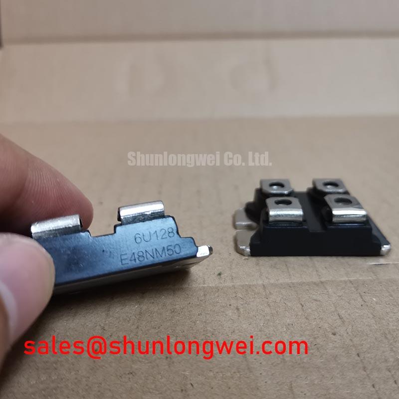
For a neutral comparison during sourcing, engineers can review the electrical role and package requirements against the CM30TF-12E. Any interchangeability decision still requires confirmation of voltage range, control interface, mechanical envelope, pin assignment, thermal path, and protection behavior from the original system documentation.
VI-252-EV Circuit Protection and Reliability: Calibrating High-Speed Fault Management
Capture the fault signal, converter output, switching-node voltage, and input current on the same time base when a servo drive reports an overcurrent or DC-bus fault. A desaturation detector, where used in the surrounding switching stage, is an external protection function and should be evaluated for blanking behavior, threshold stability, noise immunity, and the delay between detection and gate suppression. The supplied VI-252-EV data identifies the unit as a 30.0 A brick-module power supply, but does not publish a device-specific short-circuit safe-operating-area time or an internal desaturation circuit.
High-speed fault management should distinguish between a genuine short circuit, a transient current demand, sensor saturation, and a control-reference disturbance. Type-I protection can remove the gate command rapidly, while a controlled soft turn-off can reduce the voltage overshoot caused by interrupting current through stray inductance. A two-stage strategy may be evaluated when the power stage and driver support it: an initial controlled reduction limits di/dt, followed by full gate discharge. The timing and current profile must be validated against the switching devices, bus structure, driver capability, and measured peak VCE or equivalent switch voltage.
For a high-side driver using bootstrap power, verify that the capacitor can supply the required gate charge, driver quiescent current, leakage, refresh interval, and switching duty-cycle demand without excessive voltage droop. This is an engineering calculation based on the selected driver and switching device, not an official VI-252-EV parameter. The measurement should be taken at the driver supply pins during the most demanding commutation sequence, including rapid direction changes in a multi-axis servo system.
The input and output protection strategy should also account for conducted disturbances from upstream rectification and regeneration. If a phase-controlled rectifier supplies the DC link, firing-angle control, line impedance, and harmonic filtering affect the ripple presented to the converter. Gate-trigger requirements such as IGT and VGT belong to the selected thyristor and its firing circuit, not automatically to the Vicor module. The surrounding control system should verify pulse-train strength, synchronization, and isolation using the original rectifier documentation.
An auxiliary bias supply may use an active-clamp flyback topology, but that topology should be assessed as a separate circuit rather than inferred as an internal feature of this product. A useful external reference for the power-conversion principle is Active Clamp Flyback Converter for High Efficiency Auxiliary Power Supplies. Bench Diagnostic: Remove power and allow the DC link to discharge before disconnecting control or power cables.
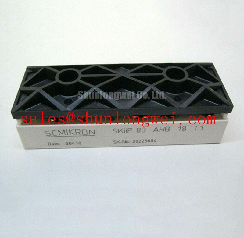
In the complete equipment chain, the Vicor converter may be evaluated alongside an upstream high-power rectifier or switching stage such as the FS225R12KE3, subject to independent confirmation of electrical compatibility and thermal coordination. The two parts should not be treated as a matched replacement set without a system-level test.
VI-252-EV Thermal-Electrical Optimization: Cosmic-Ray Robustness and Practical Voltage Derating
Measure the converter input voltage, output current, case temperature, and switching waveform at the actual installation elevation before assigning any voltage margin. The available VI-252-EV specification identifies a Standard Industrial Rating for operating voltage and a 30.0 A current rating, but it does not provide a cosmic-ray, terrestrial-neutron, single-event-burnout, altitude-derating, or FIT dataset.
Single-event effects are influenced by semiconductor technology, electric-field distribution, applied voltage, temperature, shielding, operating altitude, and exposure history. It is therefore unsafe to convert a general altitude statement into a guaranteed failure rate for this model. Designers evaluating equipment above two thousand metres should obtain applicable manufacturer reliability data where available and then verify the resulting DC-bus operating point through worst-case voltage, thermal, and transient testing. A conservative design consideration is to avoid operating continuously at the edge of the documented voltage boundary when the system can experience regenerative overshoot or uncontrolled line variation.
Voltage derating should be coordinated with load derating rather than applied as an isolated percentage. At higher ambient temperature, reduced airflow or restricted enclosure volume can increase junction and case temperature, while a lower bus voltage may require greater input current for the same output power. Measure both conditions during acceleration, deceleration, and repeated positioning cycles. A current probe and differential voltage probe can reveal whether the observed stress is steady-state loading, switching overshoot, or an upstream rectifier disturbance.
Layout remains important even when cosmic-ray exposure is not the dominant concern. Minimize high-current loop area, control the return path, provide suitable creepage and clearance, and prevent heatsink or mounting hardware from creating unintended conductive paths. The system engineer should validate insulation coordination, protective bonding, and EMC behavior at the final equipment level; a power module by itself does not constitute CISPR or EN 55011 compliance for the complete machine.
For gate-drive and switching-loop evaluation, the Precision Gate Drive Design technical resource can be used as a complementary engineering reference. Its principles should be applied together with the original Vicor documentation, the selected driver data, and measured waveforms rather than used to infer undocumented VI-252-EV internal construction.
VI-252-EV Operational Boundaries: Evaluating Thermal Capacitance and Heat-Sink Limits
Record the case temperature at the specified mounting surface while logging output current and ambient temperature through the complete pulsed workload; do not infer junction temperature from a single steady-state reading. The VI-252-EV is identified as a Vicor 30.0 A Brick Module, but the supplied data does not publish a complete transient thermal impedance curve, junction-to-case resistance, maximum junction temperature, or heat-sink interface specification.
A pulsed overload can be thermally acceptable for one duty cycle and excessive for another because the case, baseplate, heat spreader, and enclosure have different thermal time constants. Engineers may model the path with multiple RC sections, using the manufacturer’s thermal data when available, and compare the calculated junction estimate with a measured case-temperature trend. The model should include conduction through the mounting surface, interface material behavior, airflow changes, and nearby heat sources. Any calculated peak temperature is an engineering calculation, not an official product limit unless the required thermal parameters are documented by Vicor.
For a flat-mounted brick module, inspect surface flatness, interface coverage, fastener alignment, and pressure distribution. A heat spreader that contacts unevenly can produce a localized thermal bottleneck even when the average case temperature appears reasonable. If spring washers or disc springs are used, their compression range and force must be selected from the mechanical assembly specification. Do not assign a generic torque or pressure value to this model without the applicable mechanical documentation.
During troubleshooting, compare thermal behavior at constant electrical load and at constant mechanical workload. A CNC axis or robotic servo can create short regenerative pulses, repeated current peaks, and control bursts that are not visible in an averaged power reading. Correlate the converter’s output response with the drive controller’s fault log, DC-link waveform, fan state, and enclosure temperature. If the output droops only during fast motion, investigate input impedance, control-loop interaction, wiring inductance, and upstream protection before attributing the condition solely to thermal capacitance.
Thermal validation should finish with a controlled system test that includes the intended mounting arrangement, airflow direction, cable routing, duty cycle, and fault response. Designers should verify that measured voltage and temperature peaks remain within the documented limits of the converter and the surrounding power stage under both normal operation and credible transient conditions.