



Content last revised on September 12, 2026
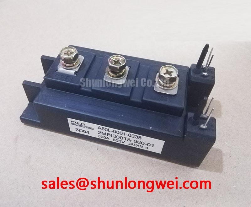
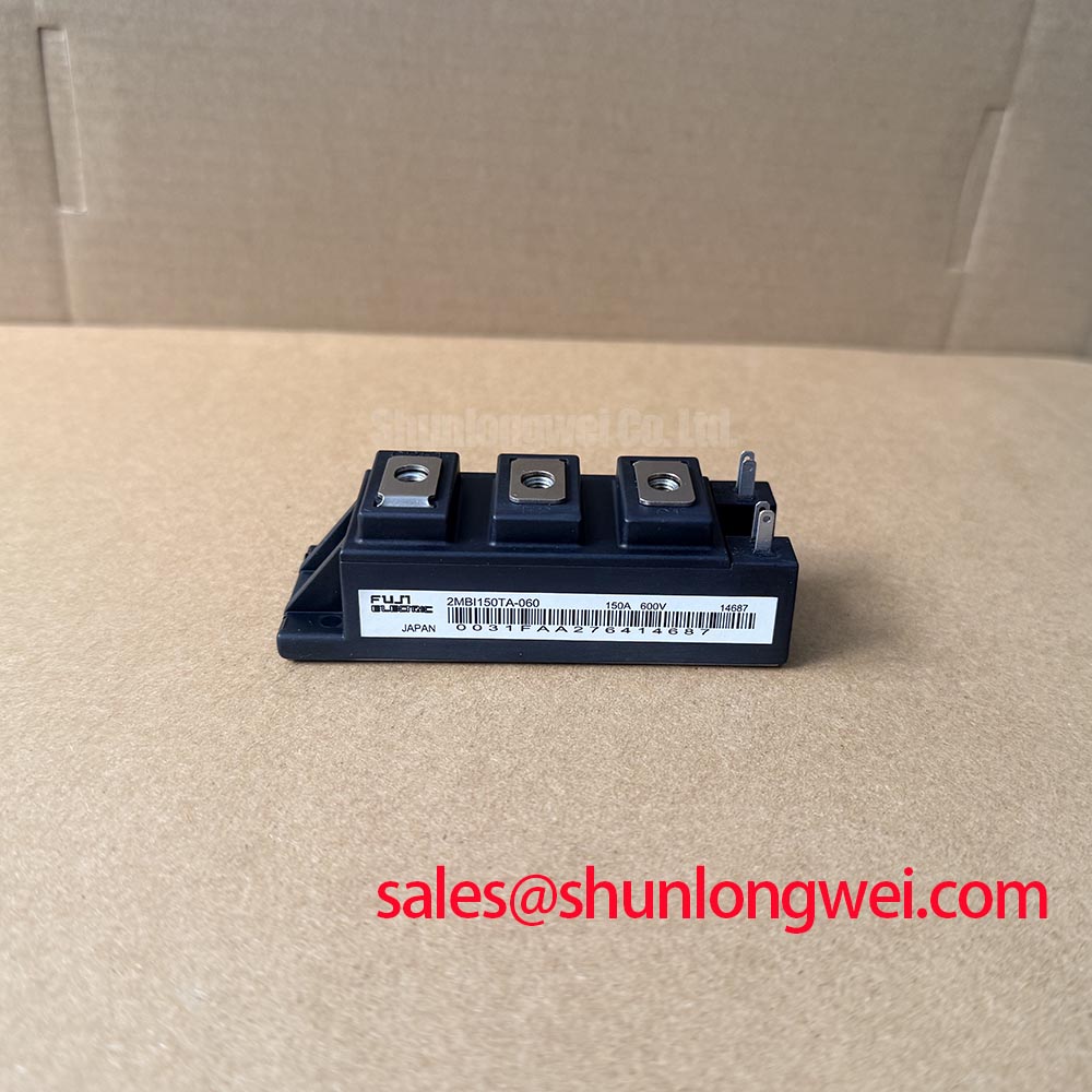
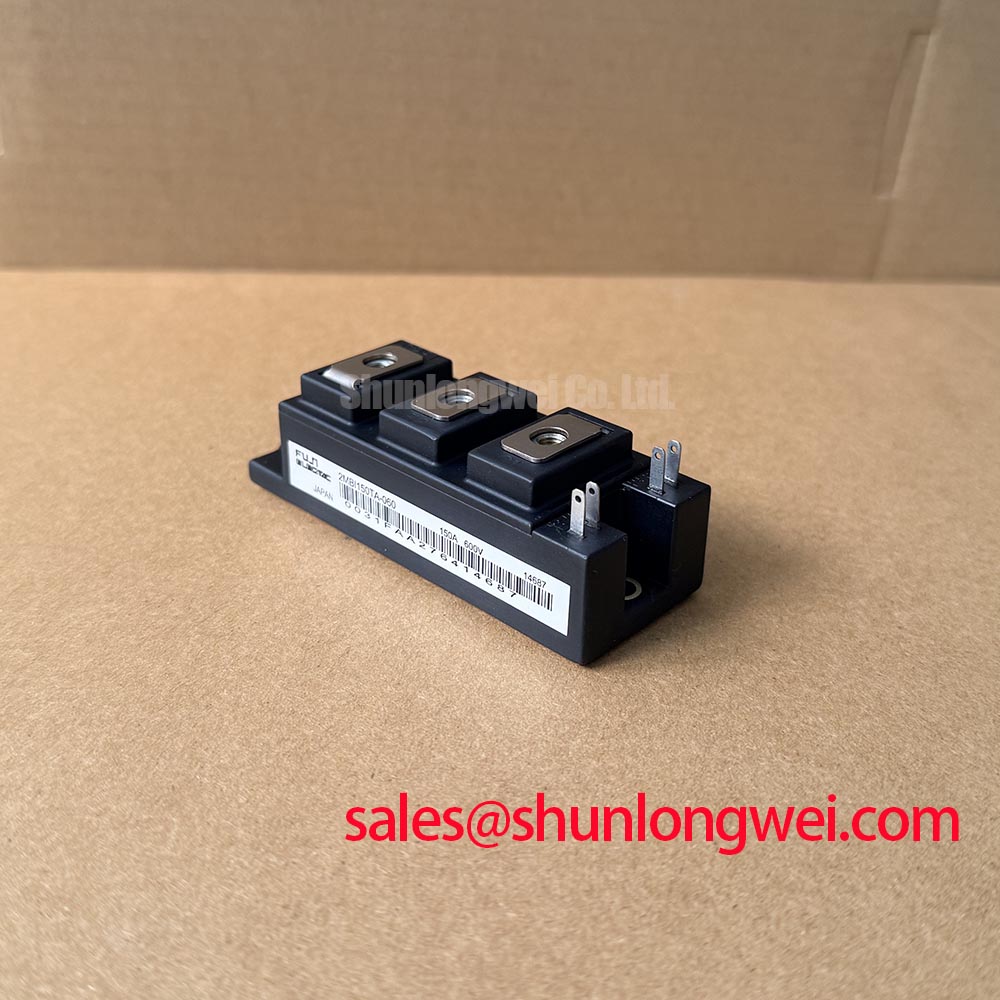
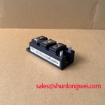
2MBI150TA-060 Specifications
| Parameter | Official Specification |
|---|---|
| Manufacturer | Fuji Electric |
| Model | 2MBI150TA-060 |
| Category | IGBT Module |
| Topology | 2-in-1 Half-Bridge IGBT |
| Collector-Emitter Voltage | 600 V |
| Collector Current | 150 A |
| Package | Fuji Power Module |
| Series | Standard |
2MBI150TA-060 Circuit Protection & Reliability: Calibrating Baseplate Thermal Grease Layer Control
Measure the temperature rise across the module baseplate and heatsink interface before investigating semiconductor failure, then inspect the thermal compound for dry areas, pump-out, contamination, and uneven compression. The 2MBI150TA-060 is a 600 V, 150 A Fuji Electric 2-in-1 half-bridge IGBT module, so its thermal path must be assessed together with switching duty, cooling airflow, and the complete power stage.
Design Consideration: A controlled TIM layer, commonly evaluated around 50–100 µm for suitable flat metal interfaces, should cover the active baseplate area without creating thick ridges or trapped air pockets. The exact material and application method remain system decisions. Clean both mating surfaces, check the heatsink for local distortion, and use a straightedge or suitable flatness inspection method before installation. If the baseplate or heatsink shows curvature, mechanical correction should provide even contact rather than relying on excess compound to fill the gap.
Use a sequential fastener pattern so pressure develops evenly across the baseplate. Confirm the assembly method, washer arrangement, and torque requirement against the mechanical documentation used for the equipment. During a service test, compare case temperature, phase-current balance, and switching waveform symmetry. An unusual VCE(sat) trend can support a thermal or drive investigation, but it should not be treated as proof of a single failed mechanism. De-saturation protection and soft turn-off should be validated at system level, including the short-circuit safe operating area conditions defined for the complete gate-drive design.
⚠️ Maintenance Note: Schedule heatsink cleaning and verify contact temperature trends after thermal-interface material aging or any fan and ducting service.
Assembly Integrity & Layout Architecture: Implementing Auxiliary Emitter Return Trace Separation for 2MBI150TA-060
With power removed, trace every gate, emitter, collector, and auxiliary return connection from the module terminals to the driver and busbar before applying a replacement part. The published product identity confirms the half-bridge topology, but the equipment drawing and the actual terminal markings must govern the field wiring. Do not assume that a nearby control return can share the same high-current path.
Design Consideration: Keep the gate-drive return physically separate from the main emitter-current route wherever the module and driver architecture provides an auxiliary emitter connection. Shared inductance can feed switching voltage back into the gate loop, which may appear as ringing, uneven turn-off, or nuisance protection operation. Minimize the high-current commutation loop, keep gate wiring compact, and validate the result with differential voltage probes at the module terminals rather than at a distant driver connector.
Inspect creepage and clearance along the DC link, half-bridge output, and gate-drive insulation paths. These distances are installation requirements determined by working voltage, pollution environment, insulation system, and applicable equipment standards; they are not inferred from the 600 V rating alone. Busbars should remain mechanically restrained under vibration, with joint surfaces free from oxide and fasteners secured according to the equipment manufacturer’s procedure.
For an inverter welder or medium-frequency induction heating supply, review the entire commutation path before changing the IGBT module. The upstream rectifier and DC-link arrangement may include a related device such as 2MBI150U4B-120; this is a topology relationship for system evaluation, not a substitute recommendation. Fuji Electric’s information on RC-IGBT Modules provides useful manufacturer-level context for power semiconductor evaluation.
2MBI150TA-060 Thermal-Electrical Optimization: Transient Thermal Impedance Practical Tuning
Capture collector-emitter voltage, gate-emitter voltage, phase current, and case temperature during the actual pulse profile when a module runs hot only during welding or induction-heating bursts. A short overload can produce a different junction response from steady-state operation, so the service assessment should compare pulse duration, repetition pattern, cooling response, and measured electrical loss.
Engineering Calculation: A transient thermal model can represent junction-to-case behavior with several RC sections, allowing each thermal time constant to respond to the measured pulse history. The resulting junction-temperature estimate should be checked against the official thermal data for the exact device revision and against the heatsink’s measured case temperature. Do not replace this verification with a generic single resistance value, particularly where battery charge and discharge cycles or repeated welding pulses create thermal cycling.
Check whether unequal gate resistance, driver supply disturbance, clamped current, or busbar asymmetry is concentrating loss in one half-bridge position. Thermal imaging can locate external hotspots, while an oscilloscope reveals whether the hot position also has a longer tail current or excessive turn-off voltage. For bidirectional DC-DC battery systems, designers should evaluate both power-flow directions and allow the control system to limit operation when thermal feedback, gate-drive quality, or cooling performance departs from the validated envelope.
Record the condition of the thermal compound during scheduled service rather than waiting for an electrical trip. A replacement comparison is meaningful only when mounting pressure, heatsink cleanliness, airflow, gate-drive settings, and load waveform are held consistent. The technical discussion in Power Electronics Masterclass can support broader selection and reliability reviews.
Transient Dynamics & Electrical Design: Transmission Line Impedance Mismatch on 2MBI150TA-060
Probe the module output and motor terminals simultaneously when long motor leads produce unexplained overshoot, ringing, or insulation stress. A reflected wave on a cable can raise the motor-end voltage substantially, and the waveform must be judged against the measured DC-link level, switching speed, cable construction, termination, and motor impedance rather than assigned a fixed multiplier.
Design Consideration: Reduce parasitic inductance in the DC-link and commutation loop to control turn-off overshoot, then verify peak VCE directly at the module during switching tests. Snubbers, output chokes, dv/dt filters, or other damping networks should be selected from measured cable behavior and semiconductor switching characteristics. Their values are system-determined; excessive filtering can increase switching loss, affect current regulation, and alter the protection response.
When the waveform differs between the module and load, check probe grounding, sensor bandwidth, busbar overlap, cable routing, and shield termination before modifying the power circuit. Confirm that the gate driver recognizes de-saturation or overcurrent conditions with the intended soft turn-off behavior, and test fault interruption at controlled energy levels. The 2MBI150TA-060 remains a 600 V, 150 A module specification; final voltage margin, filter selection, EMC performance, and short-circuit protection belong to the validated equipment design.