Content last revised on October 3, 2026
1DI150H-055 Thermal-Electrical Optimization: Thermal Cycling Margins of Internal Braking Practical Tuning
| Parameter | Available identification information |
|---|---|
| Model | 1DI150H-055 |
| Manufacturer | Fuji Electric |
| Product category | Power Transistor / Darlington Module |
| Voltage rating | Not provided in the supplied data |
| Rated current | Not provided in the supplied data |
| Package | Power Transistor Module |
Check the suspected braking path with the DC bus discharged, then compare terminal-to-terminal resistance and diode conduction against a known-good drive before removing the module. A reading that differs substantially between phases may indicate a damaged semiconductor path, an external snubber issue, or a measurement path through connected circuitry, so isolate the module before making a final assessment.
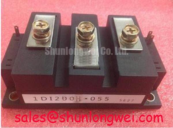
The 1DI150H-055 is identified as a Fuji Electric Power Transistor / Darlington Module in a power transistor module package. Numerical voltage and current values are not provided in the supplied data and should not be inferred from the part marking. When evaluating it in an electric forklift or warehouse traction controller, verify whether the original circuit uses this device in a braking position, a switching position, or another drive topology.
For a braking circuit, the resistor bank, switching frequency, motor inertia, DC link capacitance, and deceleration profile determine the thermal load. Designers should confirm that the resistor can absorb the expected regenerative energy while the semiconductor remains within the original electrical and thermal limits. An oscilloscope check of the DC link during controlled deceleration can reveal overshoot, repeated bus pumping, or abnormal recovery behavior without assigning a single cause prematurely.
Keep high-current braking conductors short and physically separated from sensitive base-drive or control wiring. MOVs, RC networks, or other suppression components may be present in the original design, but their selection remains system dependent. The Fuji Electric Power Semiconductor and IPM Modules resource provides useful manufacturer-level context for power semiconductor integration.
Assembly Integrity & Layout Architecture: Implementing DC-Bus Operating Voltage Headroom Derating for 1DI150H-055
Measure every power terminal against the original wiring diagram and inspect the busbar joints for discoloration, looseness, and uneven contact pressure before energizing the traction inverter. Do not assume a pin position from a visually similar module; confirm terminal identity, polarity, and auxiliary connections using the equipment documentation and continuity checks performed with the module isolated.
The listed device has no numerical DC-bus voltage, altitude derating curve, creepage value, or clearance value in the supplied factory data. Any evaluation above two thousand metres therefore requires the system engineer to review the complete insulation coordination, enclosure environment, cooling performance, and applicable semiconductor documentation. Terrestrial neutron exposure and Single Event Burnout risk should be treated as source-dependent reliability topics; no FIT rate or altitude failure prediction should be assigned without an authoritative device or system study.
For forklift and material-handling equipment, vibration can work against a poorly supported laminated busbar. Use the original mechanical fastening scheme, maintain even support around heavy conductors, and inspect for movement marks after service operation. Layout decisions should minimize commutation-loop inductance and control unintended coupling into the base-drive circuit, while switching tests verify peak voltage against the actual DC-link condition.
For a neutral comparison during replacement assessment, engineers may review the related QM200HA-HK page, but electrical, mechanical, base-drive, and protection compatibility must be verified independently rather than assumed from package appearance.
1DI150H-055 Circuit Protection & Reliability: Calibrating Fault-Clearing Dynamics: Type-I/II Desaturation
Capture the base-emitter drive signal, collector-emitter voltage, and fault output at the same time when investigating a short-circuit trip; a single alarm code cannot establish whether the initiating event was a load fault, base-drive disturbance, wiring inductance, or protection timing problem. Confirm that the protection circuit actually detects the module current path and that its fault response is compatible with the installed driver.
Type-I and Type-II desaturation arrangements are system-level protection methods, not numerical specifications established by the supplied data for 1DI150H-055. The commonly discussed sub-ten-microsecond short-circuit interval must not be attributed to this module without an applicable datasheet or test report. Designers should verify the actual short-circuit safe operating area, blanking behavior, fault propagation delay, and driver soft turn-off response using the selected base-driver documentation.
Two-stage soft turn-off can reduce the rate of current interruption and help control inductive overvoltage, but the correct sequence depends on base-drive resistance, driver capability, stray inductance, load current, and DC-link conditions. Use a properly rated differential probe and verify the measured peak against the module’s documented electrical boundary. Collector-base capacitance feedback, common-mode ground bounce, and unsuitable reverse base bias can all distort the observed waveform; these issues require circuit-level measurement rather than a fixed repair value.
The technical discussion in The 1200 V CoolSiC™ MOSFET Advantage in Three can serve as a comparative reference for switching-stress evaluation, not as a specification for this Fuji Electric module.
Benchtop Waveform Tuning: Mitigating Stress via Optimizing Heatsink Contact Pressure and Switching Behavior on 1DI150H-055
Inspect the mounting face, heatsink flatness, interface material spread, and screw seating whenever the waveform changes after replacement. A distorted baseplate contact pattern can raise thermal impedance and shift switching behavior, while excessive mechanical pressure may introduce package stress; both conditions should be checked against the original mechanical assembly instructions.
Use the specified thermal interface material and apply it consistently across the intended contact area. A nominal interface thickness such as fifty to one hundred micrometres is a general installation reference only, not an official value for this model. Designers should control voids, avoid contamination, and verify that any baseplate curvature is accommodated by the approved mounting method.
Sequential tightening is preferable to forcing one corner fully down before the others, but the required torque depends on the fastener, heatsink, washer arrangement, and manufacturer instructions. 🔧 Bench Diagnostic: Disconnect power and allow the DC link to discharge before removing terminals or changing base-drive connections.
After assembly, repeat cold resistance checks, inspect the base-drive signal at the module terminals, and perform a controlled low-energy switching test before applying full traction load. Compare turn-on, turn-off, bus overshoot, and thermal response with the original service waveform. If the system includes phase-controlled rectification, MOV protection, or harmonic filtering, evaluate those circuits together because their operating condition can alter the stress seen by the power module.