Content last revised on September 10, 2026
IEEE 61000-4-5 Industrial Surge Immunity: Metal Oxide Varistor (MOV) Integration
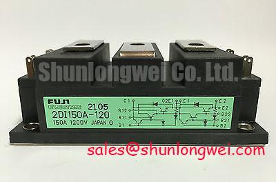
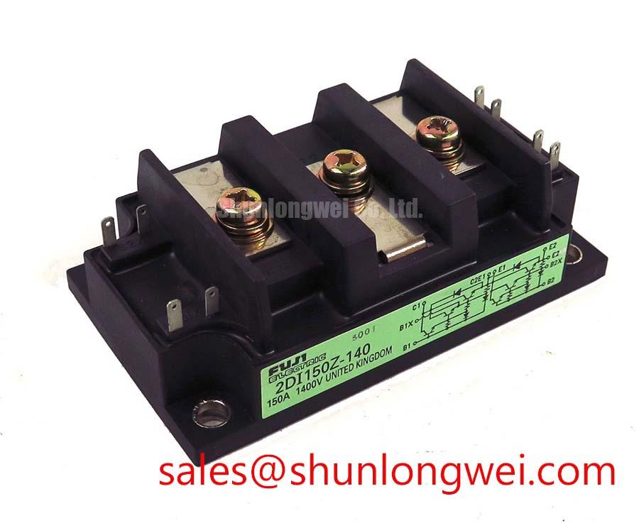
Grid-tied static VAR compensator (SVC) and thyristor-switched capacitor (TSC) assemblies interface directly with industrial medium-voltage and low-voltage distribution networks. Under standard operational mandates, these systems must endure severe transient overvoltages governed by the IEEE 61000-4-5 combination wave standard (1.2/50 μs open-circuit voltage and 8/20 μs short-circuit current). Utilizing the 2DI150A-140 from Fuji Electric, featuring a collector-emitter sustaining voltage VCEO(SUS) of 1400V and an isolation rating VISO of 2500V AC (1 min), requires front-end voltage clamping to keep transient excursions within safe electrical operating margins.
To prevent destructive avalanche conditions during line transients, metal oxide varistors (MOVs) are matched upstream of the semiconductor stage. The continuous DC and AC operating voltages define the maximum continuous operating voltage (MCOV) of the varistor network, which must be calibrated above nominal line peaks while clamping surge spikes below the module breakdown limits. In parallel with MOV arrays, RC snubber topologies absorb high-frequency transient energy. The snubber circuit limits the rate of off-state voltage rise (dv/dt), dampening parasitic oscillations caused by grid-side inductance. Maintaining proper thermal interface material (TIM) application and standardized mounting torque ensures that the junction-to-case thermal resistance Rth(j-c) remains stable, preserving device operational limits during sustained surge suppression sequences.
Evaluating Post-Surge Reverse Voltage Blocking Recovery at Elevated Junction Temperatures
When high-energy transient grid disturbances occur, the power module handles surge currents that temporarily exceed the continuous collector current IC of 150A, approaching the peak current threshold ICP of 300A. These dynamic conduction pulses generate instantaneous thermal energy within the silicon die, elevating the active junction temperature toward the absolute maximum rating of Tj = +150°C. Under such elevated thermal states, semiconductor physics dictates an increase in reverse leakage current, which directly diminishes effective breakdown margins upon immediate reapplication of blocking voltages.
Verifying the post-surge recovery envelope requires quantifying the heat dissipation path through the baseplate. If the transient energy exceeds the pulse energy capacity, localized thermal accumulation at the silicon-die interface can induce thermal runaway during the subsequent off-state voltage recovery. In comparative system designs where alternate voltage blocking ratings or differing package configurations are evaluated, engineers often review the 2DI150M-120 to analyze parametric differences across 1200V platforms. Systematic reliability protocols, thermal cycling assessments, and junction temperature validation methods are further detailed in the Field Engineer’s Handbook for power semiconductor deployment.
Gate Trigger Current (I_GT) Temperature Dependency and Back-Porch Holding Requirements
In power switching circuits and Darlington power topologies operating within static VAR systems, the base drive current IB directly influences conduction losses and switching dynamics. For the Fuji Electric 2DI150A-140, maintaining full saturation across a continuous load current of 150A requires an adequate base current up to 9A. Because current gain (β / hFE) fluctuates over the entire operating temperature span of -40°C to +150°C, drive circuitry must be designed with adequate overhead to compensate for diminished carrier mobility at low temperatures and increased leakage at elevated temperatures.
For auxiliary clamping or multi-stage converter branches within static compensation equipment, intermediate power modules like the 2DI150Z-100 are often evaluated in complementary topologies. Precise current regulation throughout wide temperature swings requires accurate real-time feedback. Implementing LEM High-Precision Current Transducers for Power Inverters provides dynamic current measurement with high galvanic isolation, enabling control loops to optimize drive pulses, suppress switching oscillations, and prevent localized hotspot formation across the silicon junctions.
Dynamic Firing Delay Angle Adjustment under Fluctuating AC Grid Voltage
Grid-tied static compensators continuously modulate reactive power injection or absorption by dynamically adjusting the conduction delay angle (α) between 0° and 150°. As the control loop modulates the firing angle in response to grid voltage fluctuations, the semiconductor components experience varying conduction periods and di/dt rise times. The resulting root-mean-square current and switching power losses dictate total heat dissipation across the heatsink assembly.
The total power loss consists of on-state saturation loss (calculated via VCE(sat) and IC) and dynamic switching losses. When α increases, peak current stresses occur over shorter duty cycles, requiring strict monitoring of junction temperature fluctuations. The mechanical and electrical specifications of the 2DI150A-140 are summarized below:
| Parameter | Symbol | Factory Rating | Unit |
|---|---|---|---|
| Collector-Emitter Voltage | VCEO(SUS) | 1400 | V |
| Continuous Collector Current | IC | 150 | A |
| Peak Collector Current | ICP | 300 | A |
| Continuous Base Current | IB | 9 | A |
| Operating Junction Temperature | Tj | -40 to +150 | °C |
| Isolation Voltage (1 min) | VISO | 2500 | V AC |
Adhering to these documented electrical parameters ensures that switching transitions remain within the defined safe operating area during rapid firing angle modulation.