Content last revised on October 1, 2026
2MPI300P-140-03 Gate Voltage Spikes: Check the Off-State Path
| Model | 2MPI300P-140-03 |
|---|---|
| Manufacturer | Fuji Electric |
| Product category | IGBT module |
| Package description | Fuji Power Module |
| Rated voltage and current | Numerical ratings were not provided in the supplied product specifications. |
Probe the off-state gate voltage during a controlled switching test and compare its spikes with the opposing switch’s voltage transitions. On a drive repair bench, a clean static gate measurement does not rule out a transient turn-on problem. Fast voltage changes can couple through device capacitance into the gate circuit; the resulting disturbance depends on the driver, return path and physical layout. Treat a spike as a waveform to investigate, not proof that the 2MPI300P-140-03 has failed.
With power isolated and the DC link confirmed discharged, compare cold gate-to-emitter resistance and terminal condition with the removed assembly’s service information. Look for loose driver connections, damaged insulation, contaminated terminals and changes in the gate return path. During energized testing, use a measurement arrangement suitable for the voltage environment and capture the gate waveform at the module-side connection where accessible. A waveform measured only at the driver board can miss a disturbance created between that board and the power terminals.
An active Miller clamp is a Design Consideration when the verified driver and module connection support it. Its purpose is to hold the gate near its off-state reference during rapid voltage transitions. A negative off-state bias is another system-level option, but its value cannot be prescribed from this product information: the allowable gate limits, driver supply and fault behavior must first be checked against the original equipment documentation. Keep the gate drive loop compact to reduce parasitic inductance, then assess whether damping changes suppress oscillation without creating unacceptable switching loss or voltage overshoot. The equipment designer determines the final arrangement from measured waveforms.
For a heavy-duty variable-frequency AC motor drive being assessed for repair, also compare the candidate module’s terminal arrangement, mounting interface and documented electrical limits with the installed part. A model name alone cannot establish interchangeability. The EVK71-060 can be placed on a cross-model comparison list, but its electrical ratings, topology and mechanical fit require independent verification before it is considered for substitution.
2MPI300P-140-03 and Regenerative DC-Bus Surges
Record the DC-bus waveform through a controlled deceleration and check whether a reported overvoltage fault follows the bus rise or a separate gate-drive event. A decelerating motor can return energy to the DC link. Whether that energy is handled by a braking chopper, a regenerative front end or another drive-level arrangement is determined by the equipment schematic, not by the IGBT module’s model number. The supplied product specifications do not establish that the 2MPI300P-140-03 contains a braking switch.
Trace the braking path on the actual drive before attributing a surge to the replacement module. Inspect the DC-link connections, braking-switch command, resistor circuit and fault log; compare their behavior with the service procedure under the same operating condition. Resistor and switch selection is an equipment design task: the permissible bus voltage, braking energy, duty pattern and thermal limits must all be established before components are sized. A higher resistor power label by itself does not demonstrate that the switch or bus remains within its limits.
If the drive uses a bootstrap supply for a high-side gate driver, check its voltage during the longest relevant high-side on-time and during recovery after a fault. As a Design Consideration, bootstrap capacitance must support gate charge and driver consumption while keeping supply droop within the driver’s operating limits. Neither the module’s gate charge nor a required bootstrap capacitor value is established by the supplied specifications, so a numerical selection would be guesswork. A low driver supply can resemble a gate or power-module fault; verify the supply waveform alongside the gate waveform before replacing either assembly.
Turn-off voltage overshoot deserves a separate check when the bus is already elevated. Keep the DC-link current path compact to limit parasitic inductance, and measure the switching peak under representative conditions against the module’s verified voltage rating. A metal-oxide varistor or another overvoltage network may form part of the equipment’s protection scheme, but its placement and energy capability must be assessed at system level. For a broader switching-test framework, see the Power Electronics Masterclass.
2MPI300P-140-03 Baseplate Contact and Thermal Interface Checks
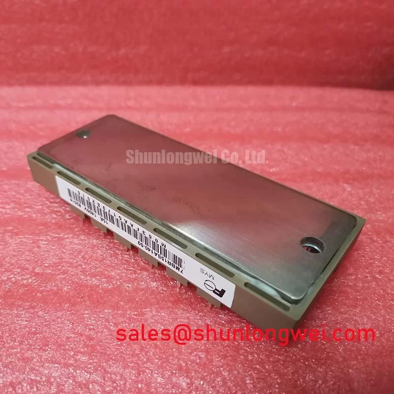
Inspect the mounting surface for old compound, burrs and uneven contact marks before seating the module. A fresh layer of thermal interface material cannot reliably compensate for debris or a distorted heatsink. Clean the mating surfaces using the equipment’s approved procedure, check that the module sits without rocking, and compare its footprint and fastener positions with the removed part. The Fuji Power Module package description alone does not establish its dimensions or mounting torque.
Apply thermal compound as a controlled, continuous thin layer rather than using excess material to fill visible gaps. As a Design Consideration, the compound and clamping pattern should promote contact while limiting trapped air and unnecessary interface thickness. Use the module and heatsink mounting instructions to set the tightening sequence and torque; those values are not supplied here. If the original assembly uses a specified pad or phase-change material, do not replace it with grease solely on the basis of appearance.
Field alert: Confirm the specified fastener torque and thermal interface method before tightening a replacement module.
After assembly, check the temperature trend under a controlled load and compare it with the drive’s prior service readings, allowing for differences in ambient conditions and cooling operation. A rapid temperature rise can have more than one cause. Inspect fan operation, heatsink passages, clamping and phase current before assigning the fault to the module. Where multiple switches share current, static and dynamic balance also depend on the verified device characteristics and on symmetrical external connections; neither balance nor parallel suitability follows from the package label.
2MPI300P-140-03 Transient Thermal Response During Overload
Capture phase current, case-temperature indication and overload duration during a repeatable test, then compare them with the drive’s protection record. A brief current peak and a sustained overload impose different thermal demands even when a display reports the same maximum current. The supplied product specifications contain no numerical current rating or transient thermal impedance curve for the 2MPI300P-140-03; consequently, they do not support a calculated peak junction temperature or a declared overload margin.
For an engineering assessment, obtain the correct manufacturer thermal-impedance and loss data for the exact device and operating conditions. An Engineering Calculation can then combine time-varying dissipation with the transient thermal response to estimate junction-temperature rise. A multi-stage thermal model is useful only when its parameters represent the relevant module and its mounting conditions. The measured case location, thermal interface and cooling response must be accounted for rather than treated as a single fixed temperature.
Inspect the gate and collector waveforms during the overload as well as the current trace. Gate oscillation, DC-bus elevation or an altered turn-off trajectory can change switching dissipation, so a thermal estimate based only on nominal current may miss the event that triggered the trip. If insulation condition is part of the equipment investigation, partial discharge is a distinct high-voltage insulation phenomenon; the partial discharge reference explains the mechanism, but it does not establish an insulation rating or test result for this module. Finish the assessment against the exact module documentation and the drive’s measured operating limits, without inferring a service-life figure from one overload trace.