Content last revised on October 23, 2026
4MBI900VB-120R1-61 Circuit Protection & Reliability: Managing Turn-Off di/dt-Induced Voltage Peaks
I check the discharged DC link and isolate the gate-driver connections before comparing collector-emitter and gate-emitter cold-state measurements across equivalent circuit positions. A resistance reading taken through connected snubbers, drivers, or parallel branches can conceal the component responsible for a shutdown. Record measurement polarity and allow capacitive readings to settle. An unexpected reading warrants circuit isolation and comparison with a known-good path; it does not establish a failure mechanism by itself.
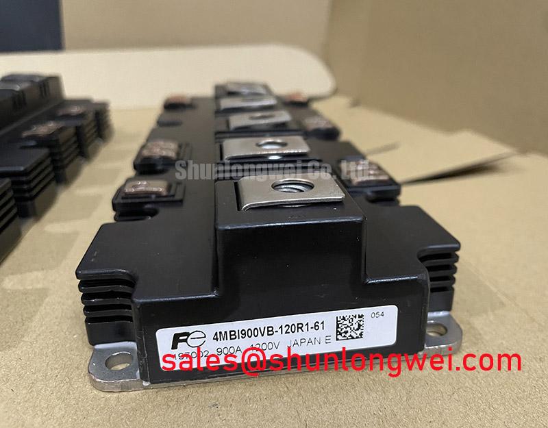
For the 4MBI900VB-120R1-61, turn-off voltage must be assessed against its 1200 V collector-emitter rating, identified here as an Official Specification. As an Engineering Calculation, the first-order relationship V_peak ≈ V_DC + L_sigma × |di/dt| explains why a short, apparently substantial busbar can still produce an excessive switching peak. This approximation describes the inductive contribution; ringing, commutation behavior, and clamp response require waveform measurement. Measure across the relevant device terminals with appropriately rated differential instrumentation and a compact probe connection.
Design Consideration: examine the complete commutation loop, including capacitor connections, terminal transitions, and return conductors. Closely coupled outgoing and returning busbar paths can reduce loop inductance when insulation and mechanical requirements are preserved. Symmetry matters where branches share current, but visual symmetry alone does not establish equal impedance. Clearance and creepage should follow the equipment insulation design, considering working voltage, environmental conditions, and the actual insulating materials; shortening a loop must not compromise those distances.
Snubber selection should follow measured overshoot, switching energy, repetition rate, and capacitor pulse capability. Positioning a suitable film capacitor near the relevant commutation terminals can reduce connection inductance, while its mounting must tolerate vibration and thermal movement. The system engineer should validate capacitance, damping, and dissipation under representative switching conditions. Mastering Power System Dynamics provides supporting context for this layout and snubber assessment.
4MBI900VB-120R1-61 Circuit Protection & Reliability: Mitigating Bolted Contact Oxidation
Measure each suspect bolted power connection with a four-wire micro-ohmmeter after isolating parallel current paths. Place the sensing contacts across the joint being assessed rather than across a length of busbar that introduces unrelated resistance. Record joint temperature, instrument conditions, and probe locations so subsequent measurements remain comparable. Differences between equivalent connections can guide inspection for surface contamination, uneven seating, damaged hardware, or mechanical strain without assigning an unsupported universal resistance threshold.
The 900 A continuous collector-current rating at Tc = 80°C is an Official Specification with an explicit case-temperature condition. It is not an instruction to run an installed assembly at that current regardless of cooling or terminal condition. During a controlled return to service, compare thermal images of equivalent joints at comparable load. Account for emissivity and reflective metal surfaces; an apparent hot spot should be checked against electrical measurements and the physical connection before attributing it to contact resistance.
Design Consideration: restore mating-surface cleanliness using the equipment-approved method and inspect terminal seating before tightening. Support the busbar so its weight or misalignment does not load the module terminal. Use the assembly-specific fastener sequence, hardware, and torque requirements. Field Alert: Use the specified tightening procedure and thermal-interface application method; extra bolt torque cannot compensate for a distorted busbar or uneven heatsink contact.
At the cooling interface, inspect flatness, surface damage, and the previous thermal-interface contact pattern. Apply the approved material uniformly using the specified assembly process; excess material and incomplete coverage both deserve investigation. Thermal-interface thickness and mounting torque belong to the particular module and heatsink assembly requirements. Pressure-contact hardware, disc springs, or double-sided cooling should be addressed only where the equipment drawings explicitly include them, rather than treated as features of this module.
When reinstalling the conductors, preserve their designed overlap, insulation placement, and snubber connection geometry. Moving a capacitor lead or bending a return conductor to relieve terminal stress can change the switching loop. Check the resulting mechanical fit before repeating the relevant transient measurements. A satisfactory cold joint measurement and an acceptable switching waveform address different failure paths; both contribute to evaluating the repaired connection.
Preventing Spurious Faults: Derating and Parameter-Mismatch Guidelines for 4MBI900VB-120R1-61
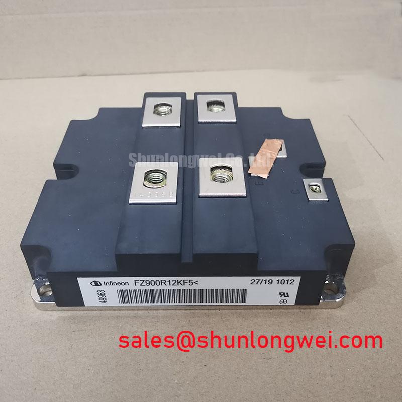
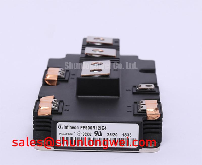
Compare the replacement circuit position, driver interface, and cooling arrangement before using a matching voltage label as the basis for installation. The 4-Pack configuration is an Official Specification, so the terminal arrangement and internal circuit connections must match the equipment schematic. For a separate component comparison, 1MBI400L-120 is a reference model requiring its own specification review; that comparison does not establish interchangeability.
The typical Vce(sat) of 1.80 V at Tj = 125°C is an Official Specification at the stated temperature, not a universal diagnostic voltage. Collector current and gate-drive conditions also affect the measured saturation voltage. Design Consideration: where parallel operation is part of the original circuit, assess current sharing using the relevant output characteristics over the intended operating region. A favorable temperature coefficient in one region does not guarantee balance throughout startup, low-current operation, or switching transitions.
Dynamic sharing requires attention to gate-loop impedance, driver timing, power-path impedance, and thermal coupling. Compare corresponding gate-emitter and collector-emitter waveforms under equivalent conditions. An unequal waveform can reflect driver behavior, connection geometry, or device characteristics, so isolate those influences before changing gate components. The Fuji Electric Power Semiconductors Portal is an appropriate manufacturer resource for identifying applicable device documentation and technical guidance.
For compatibility assessment in a utility-scale 1500 V central solar photovoltaic inverter, establish the actual blocking voltage imposed on each switching position. A 1200 V device cannot directly block a 1500 V DC link; suitability would depend on a topology that maintains each device within its limits during normal operation and relevant faults. The equipment name alone cannot establish that condition.
Design Consideration: assess desaturation detection, blanking, propagation delay, and controlled turn-off against the device’s applicable short-circuit operating limits and the existing driver design. A typical saturation-voltage value is not a desaturation threshold. Capture the protection sequence when investigating unexplained trips, including the current rise and collector-emitter response, rather than extending blanking time simply to suppress an alarm.
Preventing Spurious Faults: Kelvin Emitter Connection Guidelines for 4MBI900VB-120R1-61
Trace the gate-driver return to the emitter connection shown on the equipment schematic before moving any control wiring. Where the documented terminal arrangement provides an auxiliary emitter connection, use the designated return path as intended by the original circuit. A separate Kelvin emitter terminal is not established by the supplied headline ratings, and a convenient nearby power terminal should not be assumed electrically equivalent during switching.
Design Consideration: inductance shared by the power emitter current and gate return can alter the effective gate-emitter voltage during fast current transitions. Keep the gate and its return closely associated, minimize their enclosed loop area, and separate the control path from high-current commutation conductors where the assembly permits. These measures reduce coupling; their effectiveness should be evaluated at the module connection rather than inferred from the driver-board waveform alone.
When investigating ringing or intermittent protection events, compare the gate signal relative to the intended emitter reference at both ends of the connection. Probe placement and probe-loop pickup can create misleading differences. Check connector seating, return continuity, and routing changes introduced during service before adjusting the driver. Any gate resistance or clamp changes should remain consistent with the equipment protection strategy and be validated through controlled switching measurements.
Temperature measurements also need a defined reference. An external thermocouple follows the Seebeck effect and temperature-sensing principles, so junction placement and instrument compensation affect the reading. This does not establish an integrated temperature sensor in the module. Correlate measured case temperature with the cooling-system behavior, and use the 150°C maximum junction temperature as a device limit rather than treating a heatsink or terminal reading as the junction temperature.