
Content last revised on September 23, 2026
Fuji Electric 6MBI150U4B-170 IGBT Module: Verified Ratings and Integration Notes
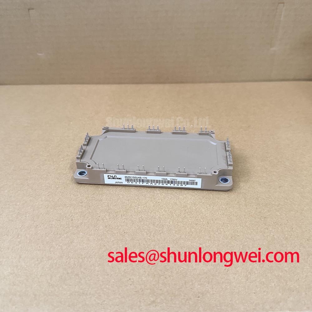
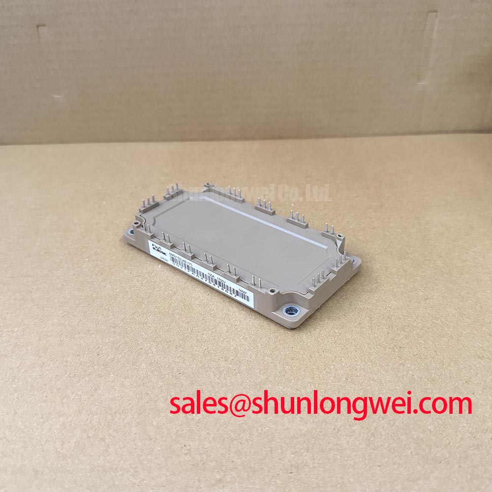
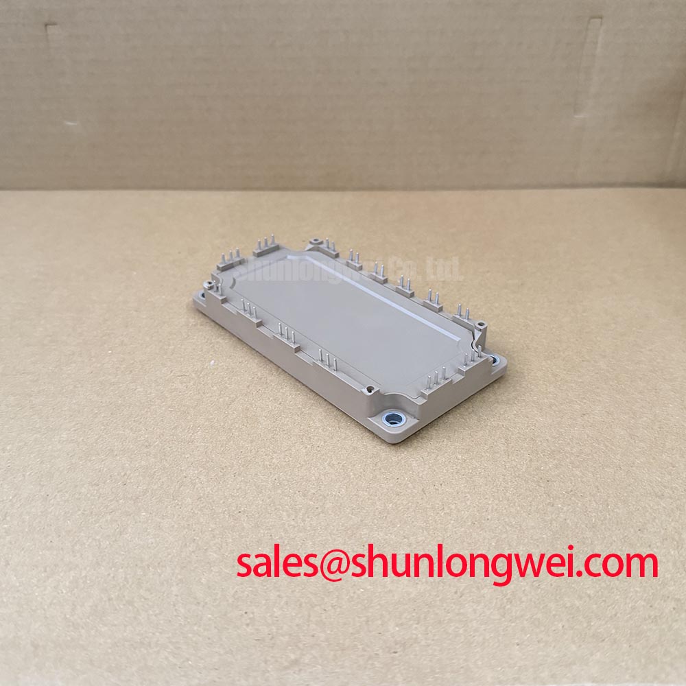
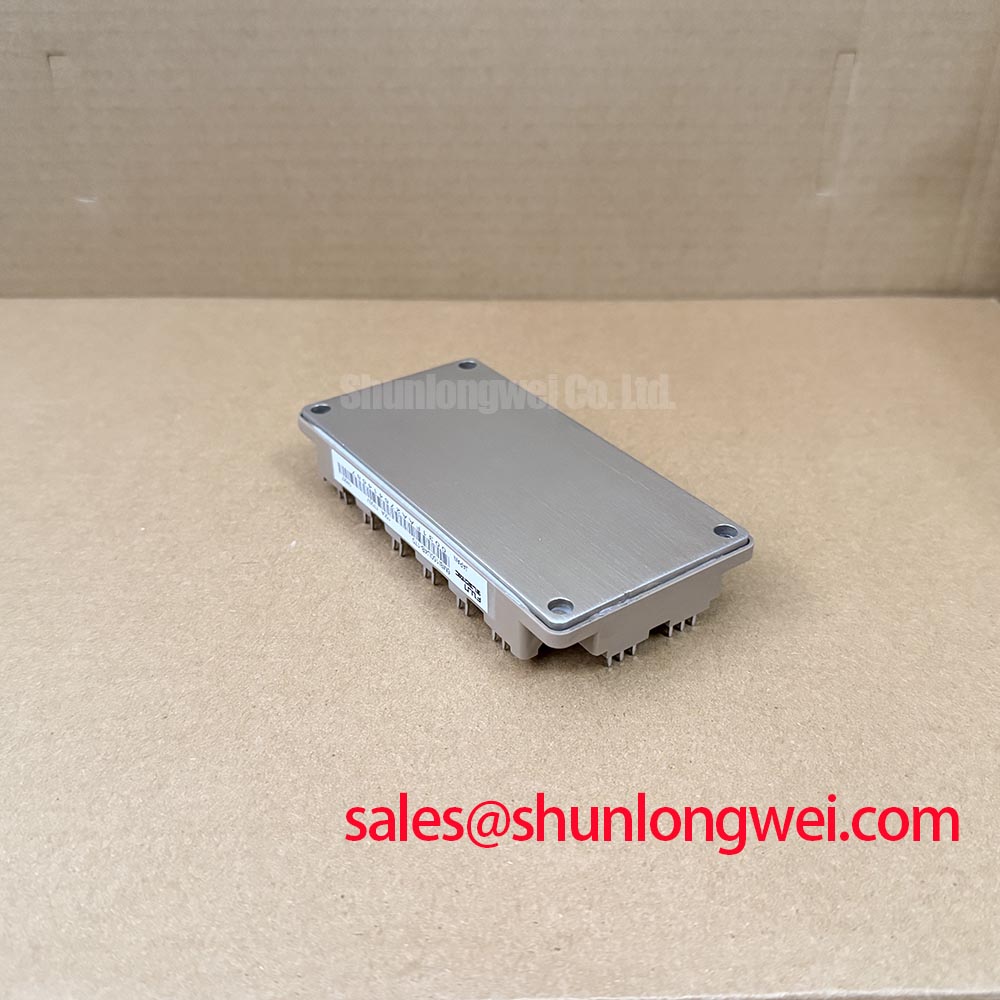
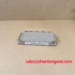
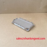
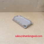
Begin a field inspection by isolating the converter, checking the module marking against the service record, and verifying the installed circuit position before applying any test voltage. The Fuji Electric 6MBI150U4B-170 is identified in the supplied factory specification context as an IGBT module with a 1,700.0 V rated voltage, a 150.0 A rated current, and a Module package. These are the confirmed product-level parameters available for procurement and initial compatibility review.
For engineers evaluating a replacement in an industrial inverter or a multi-megawatt offshore or onshore wind turbine full-scale converter, the voltage and current ratings are only the first screening points. The original circuit topology, switching frequency, DC-link condition, gate-driver interface, cooling arrangement, mechanical footprint, terminal orientation, and protection sequence should all be checked against the equipment documentation. A matching rating does not by itself establish drop-in compatibility.
| Parameter | Specification status |
| Manufacturer | Fuji Electric |
| Product model | 6MBI150U4B-170 |
| Product category | IGBT Module |
| Rated voltage | 1,700.0 V, Official Specification |
| Rated current | 150.0 A, Official Specification |
| Package | Module, Official Specification |
When sourcing for maintenance, retain the original wiring photographs and record the polarity, auxiliary connections, heatsink arrangement, and driver board relationship before removal. The product page for 6MBI150U4B-170 can be used as the purchasing reference for this specified model. Distributor information should be checked separately from the electrical approval performed by the equipment owner or service organization.
Benchtop Waveform Tuning for Hard Switching Transients on 6MBI150U4B-170
A replacement module should first be assessed with the converter disabled and the gate path disconnected from the high energy stage. Inspect the gate-emitter path, power terminals, insulating hardware, and busbar contact surfaces for contamination, looseness, or mechanical damage. Cold resistance checks can identify an open connection, an unexpected short, or an asymmetry between repeated phase positions, but they do not prove dynamic switching integrity.
During controlled commissioning, use a properly isolated double-pulse or equivalent switching test arrangement selected by the system engineer. Observe collector-emitter voltage, collector current, gate-emitter voltage, and the local supply rails with probes suitable for the switching environment. Long motor cables can behave as transmission lines. Their impedance discontinuities and termination conditions may return reflected energy toward the inverter, increasing turn-off voltage stress and producing a peak that can approach twice the incident transient under unfavorable conditions. The correct filter, snubber, clamp, or cable treatment is system-dependent and should be selected after measuring the actual waveform at the module terminals.
Short-circuit protection requires coordinated sensing, driver response, and energy limitation. A design team may evaluate Type I or Type II short-circuit detection and a response objective below 10 μs where the driver and system protection architecture support it, but this is a system design target rather than a confirmed factory parameter of this product page. The short-circuit safe operating area, pulse duration, junction temperature, DC-link condition, and gate-driver behavior must be verified from the applicable Fuji Electric documentation and the finished converter test plan.
Two-stage soft turn-off is an engineering recommendation for reducing the rate of current collapse during a detected fault. The first stage can limit the immediate voltage excursion, while the second stage completes turn-off under controlled conditions. Gate-loop inductance, driver output impedance, common-emitter layout, and the location of the fault sensor all influence the result. If the measured collector-emitter overshoot changes substantially when the probe position changes, review the measurement loop and busbar geometry before changing gate resistance.
Clearance and creepage requirements belong to the complete converter insulation system, not to the module rating alone. Designers should verify the applicable working voltage, pollution environment, altitude, insulation material group, and enclosure construction. A double-pulse test should confirm that the observed peak voltage remains within the validated system margin against the module’s 1,700 V rated voltage.
For service teams comparing physically related power-stage options, the 2MBI150UC-120 may be evaluated as a separate compatible-device candidate only after checking topology, voltage class, current behavior, gate requirements, dimensions, and thermal interfaces. It should not be treated as an automatic substitute.
Preventing Spurious Faults During Common-Mode Transients
High-side and low-side gate signals can be disturbed when the power circuit changes state rapidly. The investigation should begin at the driver output and continue to the module gate terminals, using a differential measurement method that does not introduce an unsafe reference path. Compare the command waveform, the actual gate-emitter waveform, the fault feedback signal, and the timing of the complementary channel. An unexplained pulse may indicate common-mode coupling, inadequate grounding, driver saturation, measurement error, or a damaged interface; the known-good phase position is the most useful comparison.
Reinforced galvanic isolation and common-mode transient immunity are Design Considerations for the gate-driver assembly. Values such as isolation above 5 kV or CMTI above 100 kV/μs must be confirmed from the selected driver’s own datasheet and safety documentation; they are not official specifications supplied here for the 6MBI150U4B-170. The isolator, isolated power supply, gate clamp, fault feedback channel, and PCB spacing must be evaluated as one protection barrier.
Dead-time should be established from measured turn-off delay, turn-on delay, driver propagation variation, temperature, supply tolerance, and the switching behavior of the actual circuit. A microsecond-scale buffer may be considered during initial tuning, but the correct value is system-determined. Excessive dead-time can increase conduction loss and distort current control, while insufficient dead-time can permit cross-conduction. Hardware interlock logic should remain effective even if a controller output becomes stuck or a fault signal arrives asynchronously.
Keep the gate-drive supply return physically close to the corresponding gate-emitter connection. Do not route a high-current commutation path beside sensitive fault or control traces when the board layout can avoid it. If false trips occur only at a particular load current or DC-link condition, capture the event with synchronized probes and inspect the common-mode current path rather than assuming a single defective component.
In a wind turbine full-scale converter, the front-end rectifier, DC-link protection, inverter bridge, and control cabinet interact during faults and grid disturbances. A complementary rectifier-stage device such as 6MBI450U-120A-05 can be reviewed as part of the wider topology, but its ratings and function must be validated independently from the inverter module.
Evaluating Thermal Feedback and Current-Sharing Limits
The confirmed 150.0 A rated current should not be interpreted as a guaranteed operating current under every cooling condition. Actual allowable current depends on switching loss, conduction loss, case temperature, heatsink thermal resistance, airflow or liquid-cooling performance, mounting flatness, thermal interface quality, overload duration, and the mission profile. The system engineer should establish the operating envelope using the relevant Fuji Electric thermal and electrical curves for the exact revision.
IGBT conduction voltage generally exhibits a positive temperature coefficient over portions of its operating range. As a Design Consideration, this behavior can support static current sharing between paralleled devices because the warmer path may develop a higher conduction drop. Dynamic sharing is less forgiving. Small differences in gate-loop inductance, emitter-return impedance, driver timing, busbar geometry, and thermal coupling can cause one path to conduct or switch earlier than another.
Use symmetrical power-bus geometry and matched gate wiring where parallel operation is being evaluated. Verify the current distribution with appropriate current probes during start-up, steady-state operation, load transitions, and controlled fault testing. Thermal imaging can reveal a persistent imbalance, but it should be correlated with electrical measurements because surface temperature is influenced by mounting and cooling conditions. A device that appears cooler may still experience a more severe switching transient if the measurement points do not capture the internal stress.
Before energizing a repaired assembly, check heatsink contact, insulating pads, fastener seating, and the absence of debris around the power terminals. 💡 Pro Tip: Disconnect control and power connections only after the DC link has been verified discharged according to the equipment service procedure.
For high-altitude installations, cosmic-ray, single-event burnout, FIT, and long-term lifetime claims require application-specific evidence and a defined source. No such field reliability data is established by the supplied product parameters. Designers should therefore treat altitude, repetitive overvoltage, thermal cycling, and switching stress as verification items in the converter qualification plan rather than assigning an unsupported failure-rate figure.
Dynamic Gate Impedance Control for 6MBI150U4B-170
Gate-loop impedance should be tuned from measured waveforms, not selected from a generic component list. Minimize the physical loop area between the driver, gate connection, and emitter return to reduce parasitic inductive voltage. A gate resistor or damping network can then be adjusted to balance switching loss, voltage overshoot, electromagnetic coupling, and gate-voltage ringing. The appropriate value depends on the driver strength, gate charge characteristics, PCB and busbar construction, operating temperature, and the validated switching test.
High dv/dt at the collector can couple through the Miller capacitance and lift the off-state gate voltage. A dedicated low-impedance active Miller clamp is an Engineering Recommendation for designs where measured common-emitter disturbance approaches the gate-driver threshold. Its effectiveness depends on clamp placement, isolation behavior, driver supply stability, and the actual turn-off sequence. The module’s supplied product parameters do not confirm a required negative gate bias, so any negative bias between −5 V and −15 V must be treated as a system-selected operating condition and checked against the applicable gate-emitter limits.
When ringing appears on the gate waveform, first compare the gate signal directly at the module terminals with the signal at the driver output. A difference between those locations points the investigation toward interconnect inductance, return-path impedance, probe loading, or local coupling. If both waveforms are unstable, review driver decoupling, isolation power integrity, fault feedback timing, and the commutation loop. Avoid adding damping until the source of the oscillation has been observed under the same load and DC-link conditions.
The external Fuji Electric references for Fuji Electric Brake Chopper IGBT Modules and Fuji Electric 7th-Gen X-Series IGBT Modules provide broader manufacturer-level context for IGBT application evaluation. They should not be used to infer unlisted electrical or mechanical specifications for this particular model. For a wider comparison of switching-device technology and converter topology, engineers can also consult The 1200 V CoolSiC™ MOSFET Advantage in Three.