
Content last revised on October 11, 2026
Field Diagnostics & Commissioning: PCB Symmetry Considerations for IGBT in 6MBI50F-060 Topologies
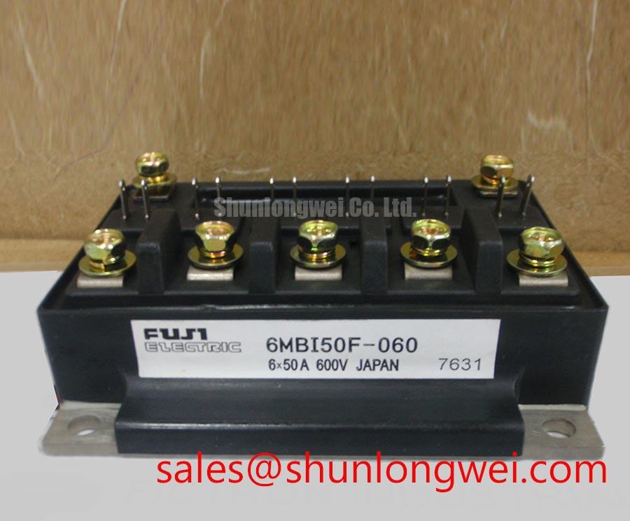
With the DC link isolated, I first verify the marked power terminals and gate connections against the service drawing, then compare cold-state readings with an electrically known-good module before connecting the control board. The 6MBI50F-060 is identified here as a Fuji Electric IGBT module rated at 600.0 V and 50.0 A, in a Fuji Power Module package. These are official product specifications; switching frequency, gate voltage, short-circuit capability, isolation performance, and thermal limits require the applicable device documentation and system test conditions.
For an IGBT power path, the main emitter return and any auxiliary or Kelvin emitter return should be treated as separate current paths. The high-current emitter trace carries commutation current and its voltage changes with parasitic inductance. Where provided, the auxiliary return should instead reference the gate-driver sensing point with minimal exposure to the power loop. Joining both returns at an arbitrary copper area can inject emitter movement into the gate signal, producing apparent gate ringing, uneven switching, or intermittent driver faults.
A practical commissioning check is to trace each gate loop from the driver output to the module terminal and back to the driver reference. Keep the gate path compact, avoid routing it beside the collector bus, and maintain consistent geometry between complementary switching paths. The control reference should not share a narrow neck of copper with the high-current emitter route. Where the existing board uses a common return, inspect solder joints, vias, terminal screws, and copper neck-down points before changing the gate resistor. A damaged connection can resemble a semiconductor problem during a cold resistance check.
The first powered test should use a controlled DC-link condition and a current-limited setup. Probe the gate-to-emitter voltage directly at the module terminals rather than at the driver IC. Compare the two switching channels for timing, overshoot, and settling behavior. If one channel shows substantially different ringing, examine the physical return path and probe grounding arrangement before concluding that the module is electrically mismatched. A long oscilloscope ground lead can create a false waveform and should not be used for high-speed gate measurements.
Designers evaluating a replacement should compare terminal arrangement, mounting geometry, gate-drive polarity, and the original protection sequence. The 2MBI400TB-060-02 is a separate Fuji Electric IGBT module that may be reviewed for topology comparison, but its electrical and mechanical characteristics must be matched independently rather than assumed interchangeable with the 6MBI50F-060.
At high altitude or in installations exposed to increased cosmic-ray activity, single-event burnout and voltage derating become system-level reliability considerations. No FIT rate, SEB threshold, or altitude life figure should be assigned to this module without an authoritative device source and the actual DC-link, temperature, switching, and protection conditions. The useful field action is to record peak collector-emitter voltage during the real switching event and evaluate the result against the approved design margin. Creepage, clearance, contamination, and enclosure conditions also belong to the complete assembly assessment, not to the 600.0 V nameplate value alone.
Benchtop Waveform Tuning: Mitigating Stress via Diode Softness Factor Optimization on 6MBI50F-060
Reverse-recovery behavior should be assessed at the commutation point where the antiparallel diode hands current back to the opposing IGBT. The important observations are the diode reverse-recovery current, the sharpness of its recovery slope, collector-emitter overshoot, and the interaction between these events and the gate-drive loop. A sharp recovery transient can increase conducted and radiated emissions, while excessive gate damping can increase switching loss. The correct balance depends on the complete power stage.
Use a double-pulse or equivalent controlled switching arrangement only after confirming probe bandwidth, loop inductance, current-sensor orientation, and safe operating boundaries. Record the collector-emitter waveform at the module terminals, not at a remote DC-link capacitor. The wiring between capacitor, module, and return bus forms part of the commutation loop; changing that wiring can change the measured peak even when the semiconductor remains unchanged.
For phase-angle conduction or servo inverter evaluation, line-frequency ripple on the DC link can alter the current at which reverse recovery occurs. Smooth the test supply sufficiently for repeatable comparison, then vary load current and switching timing separately. This prevents a ripple-related change from being mistaken for a diode softness change. The gate signal should be monitored at the module pins so that driver delay, common-emitter inductance, and actual turn-on timing remain visible in the same record.
An RC snubber is a Design Consideration for controlling a repeatable high-frequency transient, not a universal cure for every overshoot. Select its structure from measured ringing frequency, damping behavior, capacitor voltage stress, resistor pulse capability, and resulting power loss. The snubber should be placed across the switching node or device terminals with a physically short loop. A remote snubber connected through long traces may reduce the visible waveform at one location while leaving the semiconductor exposed to a different local peak.
Turn-on gate resistance can also be used as a Typical Starting Point for bench tuning. Increase damping only while checking switching loss, junction-temperature rise, diode recovery interaction, and current-sharing behavior. Do not infer a suitable resistance from the 50.0 A rating alone. The driver supply, gate charge, bus inductance, load current, and operating temperature determine the final setting. The 2MBI100N-060-10 may appear elsewhere in a related rectifier or power-conversion topology, but its presence does not establish a gate-drive setting for the 6MBI50F-060.
Long motor cables add another measurement challenge in precision stepper and BLDC servo actuator systems. The cable behaves as a distributed network, so a fast edge can reflect from the motor end and return toward the inverter. The resulting voltage may produce a two-times peak relationship at particular terminations, but the actual amplitude depends on cable construction, length, motor impedance, switching edge, grounding, and installation layout. Designers should verify the motor-terminal waveform, evaluate filtering and common-mode behavior at system level, and confirm that any filter does not compromise control-loop response or device switching conditions.
Fuji Electric’s information on RC-IGBT modules and brake chopper IGBT modules provides useful context for comparing integrated power-conversion functions. Those product families should not be treated as evidence of identical reverse-recovery behavior or pin compatibility with this module.
6MBI50F-060 Thermal-Electrical Optimization: Thermal Paste Degradation Prevention and Mechanical Tuning
Thermal performance depends first on the contact between the module base and the heatsink. Remove old interface material completely, inspect both surfaces for burrs or local contamination, and apply a thin, continuous TIM layer that covers the working area without trapped voids. A 50–100 µm process window can be used only as a Design Consideration where the selected material and assembly process support it; it is not an official 6MBI50F-060 rating. The material supplier’s spread method, pressure behavior, and temperature range remain controlling factors.
Baseplate curvature and heatsink flatness should be checked when a module shows uneven thermal behavior across repeated assemblies. Excessive mounting pressure at one corner can reduce contact elsewhere, while insufficient pressure can leave visible voids in the interface layer. Use the manufacturer’s specified fastener sequence and torque for the actual module and heatsink combination. Tighten progressively in a cross-pattern so the baseplate seats evenly, then inspect for movement or displaced compound before applying full operating power.
⚡ Safety Interlock Note: Isolate the DC link and verify discharge before touching the module terminals, gate wiring, or heatsink fasteners.
Thermal-electrical verification should combine heatsink temperature, phase current, switching waveform, and gate behavior. A rising case temperature with stable current can point toward interface degradation, airflow change, mounting distortion, or increased switching loss; it does not identify one cause by itself. Compare the repaired assembly with its original thermal profile under the same load sequence, and inspect the hottest switching position rather than relying only on an enclosure sensor.
When this module is evaluated for a precision stepper or BLDC motor servo actuator, the system integrator should verify the original control topology, terminal assignment, gate-driver protection, braking arrangement, motor-cable filter, and enclosure insulation. Minimize commutation-loop area, keep auxiliary gate-return paths away from high-current copper, and validate peak electrical stress after the final mechanical assembly. The engineering guide on IGBT Design & Integration can be used alongside the module documentation when reviewing gate drive, thermal management, and circuit topology decisions.