


Content last revised on September 30, 2026
6MBP30RTB060-50 Thermal-Electrical Optimization: Transient Thermal Impedance Practical Tuning
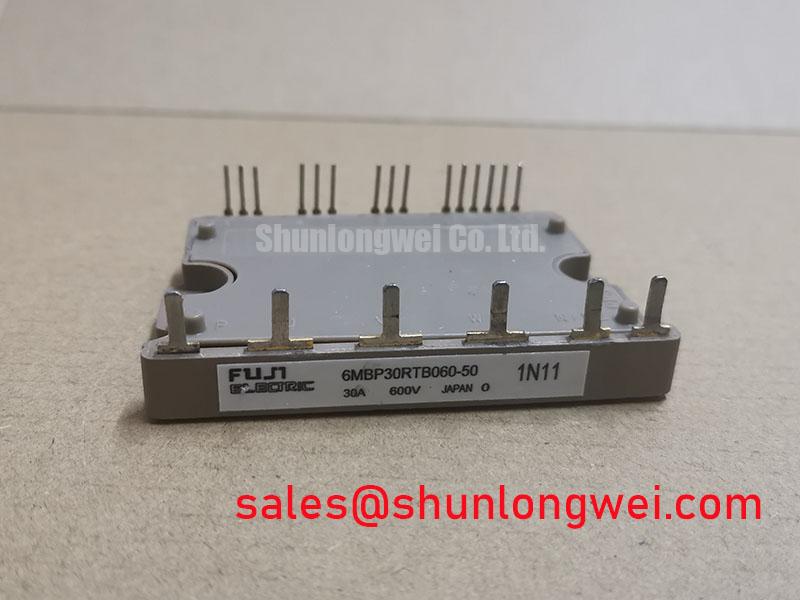
Probe the case temperature, DC link, phase current, and switching waveform together when an installed 6MBP30RTB060-50 shows intermittent thermal alarms or shutdowns under pulsed load. A single surface temperature reading cannot identify whether the limiting condition is semiconductor junction heating, mounting resistance, inadequate airflow, regenerative energy, or a switching transient that increases instantaneous loss.
The device is specified at 600.0 V and 30.0 A as the supplied official product parameters. Those ratings define the component identity and electrical boundary, but they do not by themselves establish an allowable combination of voltage, current, switching frequency, duty cycle, case temperature, and overload duration. The operating point must therefore be checked as a combined electrical and thermal condition during the actual inverter cycle.
For transient analysis, use the manufacturer’s junction-to-case thermal impedance information when available and represent the response as a multi-RC network in the thermal model. The first network sections describe rapid junction heating during a switching pulse, while slower sections represent heat spreading into the baseplate and heatsink. A model that uses only steady-state thermal resistance can miss the short-duration junction temperature rise caused by acceleration, spindle loading, regenerative braking, or repeated current pulses.
When a compact industrial inverter enters regenerative braking, the switching devices and braking path can dissipate energy in a different pattern from motoring operation. Check the DC-link voltage during deceleration, the braking command, the pulse repetition pattern, and the cooling response after the event. A brake resistor or chopper stage should be evaluated as part of the complete energy path rather than treating the IPM as an isolated heat source. The available product information does not establish a specific braking-energy capacity for this model, so the system designer must calculate the energy absorbed by the selected braking circuit and verify the resulting voltage and temperature waveforms.
Mounting condition is equally important. Inspect the baseplate contact area for contamination, uneven pressure, damaged flatness, or excessive thermal-interface material. The heatsink should present a mechanically stable surface, and the mounting sequence should distribute pressure without distorting the module. Keep power terminals, control wiring, and cooling hardware accessible for inspection after installation. Airflow should be measured at the heatsink location under the enclosure condition in which the inverter will operate, because a laboratory fan position may not represent the final cabinet flow pattern.
Use a controlled load test to separate thermal accumulation from an electrical overshoot problem. Record case temperature and current over repeated operating cycles, then compare the waveform at low and high load. A temperature rise that continues after current has returned to a lower level can indicate stored thermal energy in the module and heatsink. A rapid trip that occurs with little case-temperature change may instead require examination of gate-drive behavior, desaturation protection, DC-link overshoot, or control-board noise.
Benchtop Waveform Tuning: Mitigating Stress via High-Speed Fault Management and VCE Desaturation
Capture the collector-emitter waveform and gate-emitter waveform at the module terminals when a fault, pulse-width anomaly, or unexplained inverter shutdown occurs. Use a properly rated differential probe and a short measurement loop, then compare the affected phase with a known-good phase under the same load command. The objective is to establish whether the protection circuit is responding to a genuine overcurrent event, a switching transient, or a noisy gate-drive reference.
Desaturation protection can provide a fast response to abnormal conduction, but the applicable detection delay, blanking interval, fault-current threshold, and soft turn-off behavior are system-specific unless explicitly stated in the manufacturer’s documentation. Do not assign a fixed short-circuit withstand time to the 6MBP30RTB060-50 from the part number alone. Confirm the installed driver’s type-I or type-II protection behavior and test the complete path, including the isolated supply, fault latch, reset logic, and controller response.
A practical bench sequence begins with a reduced-energy DC link and a current-limited test condition. Observe the gate command at the driver output, the gate voltage directly at the module interface, and the collector-emitter response during turn-on and turn-off. Gate-loop inductance can create a difference between the driver reference and the module emitter reference. That difference may produce false protection activity or insufficient gate control, particularly when high di/dt current flows through a shared return path.
Keep the power-current loop and the gate-drive return physically separated wherever the module interface permits. If the module provides an auxiliary emitter or separate control return, route that connection as a dedicated sense path and terminate it according to the original drive architecture. Do not assume that a control terminal can share a high-current emitter trace without affecting the measured gate voltage. The correct connection depends on the module pin arrangement, driver topology, isolation method, and board layout.
Two-stage soft turn-off can reduce the electrical stress produced when a faulted device is forced off, but the timing and gate-current profile must be tuned against the actual DC-link inductance and fault current. A turn-off sequence that is too aggressive can increase inductive voltage overshoot; one that is too slow can prolong abnormal conduction. Verify the peak collector-emitter voltage, gate waveform, current decay, and driver supply behavior on an oscilloscope before enabling full-energy operation.
Switching-frequency derating must be established from measured semiconductor loss, heatsink performance, ambient temperature, and operating duty rather than from a generic frequency label. For a compact inverter or high-speed CNC spindle drive, compare the thermal result at the intended acceleration, constant-speed, and deceleration patterns. Also inspect whether a high-ambient cabinet condition changes the fault waveform through driver supply variation or increased junction temperature.
Fuji Electric’s High-Speed Discrete IGBTs reference material provides useful background on switching behavior and power-semiconductor application considerations. It should be used as technical context rather than as a substitute for the exact gate-drive and protection data applicable to this Fuji Power Module.
6MBP30RTB060-50 Transient Dynamics and Electrical Design: High-Frequency Commutation Loop Inductance
Measure the turn-off voltage directly across the power terminals and correlate it with the current fall time when the inverter produces an overvoltage alarm or abnormal motor noise. A long probe ground lead can create a false spike, so use a spring connection or a suitable differential measurement method positioned at the module terminals. Compare the measured waveform with the DC-link voltage and repeat the test at more than one load condition.
Commutation-loop inductance converts a rapid current change into an additional voltage transient. In engineering terms, the peak voltage rises with both loop inductance and di/dt, so the useful design action is to minimize the high-current loop area and then verify the remaining peak against the device voltage boundary. The exact permissible switching overshoot is determined by the complete system, including the DC-link operating range, parasitic inductance, gate resistance, load current, switching temperature, and protection clamp.
Use a compact and symmetrical busbar arrangement between the DC-link capacitor, module power terminals, and commutating path. Keep the forward and return conductors close together, avoid unnecessary routing around control boards, and prevent high-current paths from crossing sensitive gate or current-feedback traces. The physical layout should also leave adequate clearance for insulation, probing, maintenance access, and the voltage category of the finished assembly.
Snubber selection should follow measured waveform energy and ringing frequency. A capacitor added without checking its current pulse, dielectric behavior, mounting inductance, and resistor dissipation can shift rather than remove the transient. Start from the measured ringing signature, identify whether the dominant loop is inside the power stage or outside it, and then validate the selected network under the highest relevant current and DC-link condition. The supplied official parameters do not provide a specific snubber capacitance or loop-inductance limit for this model.
Gate resistance affects the tradeoff between switching loss, voltage overshoot, electromagnetic disturbance, and fault response. Any adjustment should be made at the driver and module interface while monitoring gate voltage, collector-emitter voltage, current, and case temperature. A value that appears acceptable at light load may produce a different result during regenerative braking or high-speed spindle acceleration.
Parallel-device applications require particular attention to both static and dynamic current sharing. Positive temperature coefficient behavior can support current balancing in some operating regions, but it does not remove the need for matched electrical paths, symmetrical gate-drive routing, and consistent thermal contact. Verify current sharing with appropriate current probes and examine turn-on and turn-off timing for each parallel path. Do not infer balanced dynamic current from equal control commands alone.
Pro Tip: Keep the DC-link capacitor, module terminals, and commutation path physically compact, then confirm the remaining voltage margin with a properly connected differential probe during the real switching test.
For a broader comparison of power-conversion device technology, the related The 1200 V CoolSiC MOSFET Advantage in Three article can be consulted as a technology reference. It does not change the specified ratings or integration requirements of the 6MBP30RTB060-50.
6MBP30RTB060-50 Circuit Protection and Reliability: Calibrating Output Sinusoidal Filter versus dv/dt Reactor
Check the motor-terminal waveform at the inverter output and at the motor when a compact drive shows insulation stress, audible ringing, overcurrent trips, or elevated bearing-current concerns. Measure with the motor cable installed at its intended length and routing, because the cable, motor input network, grounding arrangement, and output filter form one transmission path.
A long motor lead can create impedance mismatch and reflected-wave behavior, increasing the voltage seen at the motor terminals above the inverter output waveform. The magnitude depends on cable construction, termination, motor impedance, switching edge rate, installation geometry, and DC-link condition. A general statement about a fixed multiple of DC-link voltage should not be applied to every installation. Verify the actual terminal peak and rise time before selecting a filter or reactor.
A sinusoidal output filter changes the waveform toward a motor-friendly low-frequency voltage, but it also introduces capacitance, inductance, losses, resonance behavior, and possible control-loop effects. A dv/dt reactor primarily limits edge rate and can provide a different compromise between motor protection, filter size, voltage drop, and switching loss. The selection should follow the motor insulation requirement, cable length, drive control method, carrier behavior, and measured terminal waveform.
When integrating this module into a high-speed CNC spindle drive, check whether the output network remains compatible with the drive’s current sensing and protection thresholds. A filter can alter current phase, transient response, and fault-current development. Test acceleration, steady operation, rapid deceleration, and commanded stop with the final motor cable and grounding configuration. If the drive uses regenerative braking, observe the DC-link during the same sequence because output filtering does not resolve excessive energy returning to the link.
Front-end topology also matters when evaluating the complete power stage. The related 6MBI50FA-060-01 may be reviewed as a neutral reference for a front-end or complementary power-stage component, subject to voltage, current, topology, thermal, and mechanical compatibility checks. It should not be treated as an automatic replacement or guaranteed companion for the 6MBP30RTB060-50.
For field troubleshooting, compare the inverter-side and motor-side waveforms, inspect filter-component temperature, check shield termination and protective-earth continuity, and review the gate-drive waveform after any output-network change. A fault that appears only with a particular cable or motor may indicate an interaction among the switching edge, cable impedance, filter resonance, and grounding path rather than a single failed module. Record the DC-link voltage, phase current, switching command, and protection status at the same time so that the replacement decision is based on repeatable evidence.
For a related device evaluation, engineers can place 6MBP75NA060 beside this model for a neutral parameter comparison, while checking the required voltage class, current rating, package, terminal arrangement, gate-drive requirements, thermal interface, and controller protection compatibility. Mechanical fit or a similar product name does not establish electrical interchangeability.