Content last revised on September 17, 2026
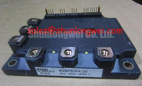
Assembly Integrity & Layout Architecture: Evaluating Thermal Capacitance vs Heat Sink for 6MBP50RJ120
The 6MBP50RJ120 must transfer heat consistently from its baseplate into the equipment heat sink before any switching test is attempted. Clean away aged interface residue from both mating surfaces, inspect for scratches or raised debris, and confirm that the heat sink remains flat across the module footprint. A dry area, uneven paste spread, or an assembly surface distorted by old hardware can create localized thermal resistance even when the external heat sink appears substantial.
Thermal capacitance and heat sink mass do not by themselves establish a safe pulsed load condition. During a short overload, junction temperature responds through the module’s internal thermal path before the larger heat sink has time to absorb much energy. The applicable transient thermal impedance curves, load pulse shape, initial case temperature, switching losses, and conduction losses must therefore be reviewed together. This is a Design Consideration; no pulse capability, junction temperature margin, or transient thermal resistance value is asserted here because those values are not included in the supplied official parameters.
Where the original equipment thermal model uses a multi RC network, the service engineer can enter the manufacturer provided transient thermal data and calculate the estimated junction rise from the actual dissipation waveform. The resulting estimate should then be verified with measured case temperature and controlled electrical loading. A sudden rise in heat sink temperature, repeated thermal protection activity, or unequal heating among phases may point to several conditions, including interface degradation, altered airflow, excessive switching stress, or a gate drive issue. It should not be assigned to one cause without measurement.
As a general installation Design Consideration, a thin and continuous thermal interface layer is preferred to avoid insulating voids while preventing excessive material buildup. If the equipment uses M5 fasteners, 2.5 to 3.5 N·m is a general industry mounting reference rather than a Fuji Electric specification for this module; the equipment drawing, screw grade, washer stack, and heat sink material determine the final approved torque. Tighten progressively in a balanced pattern and recheck that terminal busbars do not introduce mechanical strain after mounting.
Commercial string inverter and micro grid energy storage equipment can experience broad load variation, but that application context does not establish a module specific duty rating. When assessing a repair, compare the original heat sink arrangement, fan condition, air channels, busbar placement, and thermal interface method with the existing installation. For practical review of switching loop, gate drive, and thermal integration principles, see IGBT Design & Integration.
6MBP50RJ120 Operational Boundaries: Evaluating Cosmic Ray Robustness and Voltage Derating Limits
The official voltage identity available for this unit is VCES = 1200V. Before installation, verify the actual DC link voltage, recorded overshoot during switching, protection response, and the intended operating envelope against the original equipment design. The collector emitter rating is not a direct instruction for selecting a DC bus value, because switching transient amplitude depends on busbar inductance, capacitor placement, load current, commutation behavior, and gate drive conditions.
Altitude and terrestrial neutron exposure can be part of a system level reliability assessment, especially when equipment is deployed beyond the environmental conditions used for its original design validation. No quantified cosmic ray robustness, single event burnout rate, FIT result, altitude derating curve, or lifetime estimate is provided in the supplied module specifications. Those figures should not be inferred from the 1200V rating. A Design Consideration is to obtain application qualified evidence from the equipment designer or a relevant manufacturer source before assigning the module to an elevated altitude or high availability installation.
Gate drive source and sink current must be established from the actual driver capability, gate network, module data, measured switching waveform, and protection coordination. An external gate resistor can damp ringing, but its final selection is system determined: it must control overshoot and oscillation without undermining switching loss, timing, or fault response. Measure gate emitter voltage and collector emitter behavior using appropriate probing practice during commissioning. If waveform differences appear after replacement, inspect the driver supply decoupling path, connector seating, return routing, and power loop geometry before altering component values.
The pre driver supply specification is 15.0V typical and 20.0V maximum. Verify supply polarity, regulation, startup behavior, and ripple at the module side of the harness under actual operating conditions. Do not substitute a presumed drive voltage merely because it is common in another inverter platform. For a related Fuji Electric module being considered during a documented engineering comparison, the 7MBR50SB120-01 should be evaluated only against its own documentation and the host system’s electrical and mechanical requirements.
Transient Dynamics & Electrical Design: Thermal Stress Alleviation in Bidirectional Operation for 6MBP50RJ120
In a bidirectional battery linked converter, energy can move from the DC battery rack toward the AC side and return toward the DC link depending on operating mode. The direction of real power flow changes conduction paths and commutation conditions, while cyclic loading can change the thermal stress pattern across the converter assembly. The 6MBP50RJ120 should be assessed as part of that complete topology, not by voltage rating alone.
Start with the existing converter schematic and identify which module terminals participate in each active power path. Compare phase current records, DC link voltage, switching frequency configuration, control mode, and protection logs before and after service. If temperature excursions are observed during peak shaving or battery charging, collect synchronized measurements rather than treating current direction as the sole explanation. Load imbalance, DC link capacitor condition, cooling restrictions, gate timing variation, and control instability can all affect thermal behavior.
DC link capacitors are electrically close to the switching loop and influence how the converter manages pulsating current. Their selection, condition, connection resistance, and physical placement remain system design matters. Engineers reviewing capacitor technology and product information can consult Nichicon inverter grade aluminum electrolytic capacitor resources; that reference does not certify compatibility with this specific Fuji Electric module or a particular inverter design.
Keep high current paths compact and mechanically supported so that busbar movement, loose joints, and unnecessary loop area do not add uncertainty during switching. The principle is to minimize parasitic loop inductance where turn off overshoot must be controlled, then verify peak voltage margins against the DC link voltage through instrumented switching tests. Check DC link connections with power removed, inspect capacitor terminals for heat evidence, and use the original service procedure for discharge confirmation before touching the power stage.
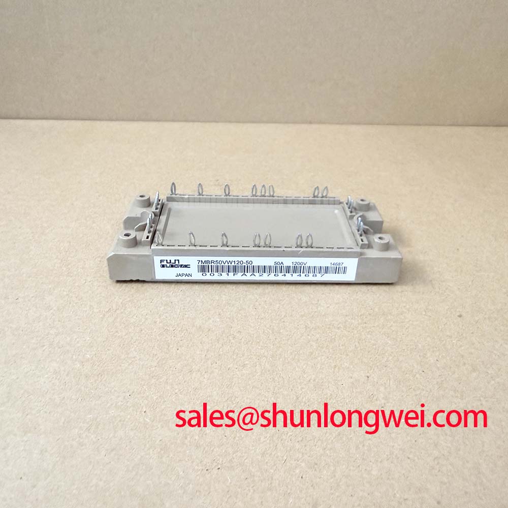
Where a rectifier or complementary stage is being reviewed as part of the same equipment repair, 7MBR50SA120-50 is a related item that can be documented separately. Its presence in a comparison does not establish interchangeability, electrical equivalence, or suitability for the 6MBP50RJ120 installation.
Preventing Spurious Faults: Optimizing Gate Drive Loop Geometry and Pre-Driver Guidelines for 6MBP50RJ120
Spurious fault activity after a power module change often warrants a careful inspection of the gate drive loop before blaming the module. Trace the driver output, control connector, local decoupling capacitors, return path, and protection feedback against the original layout. Long parallel routing beside high current conductors can couple switching noise into sensitive control paths. Keep the drive loop compact, keep its reference path intentional, and avoid sharing a sensitive control return with a large pulsed power return wherever the circuit design provides separate connections.
Some inverter assemblies use an auxiliary emitter reference or equivalent low current return at the control interface. The original schematic and module pin documentation must confirm whether and how that connection is used for this model. Where the equipment provides a separate sensing return, route it as the driver reference rather than extending it through the main emitter current path. This is a Design Consideration based on common gate drive practice, not a claim about undocumented internal construction of the 6MBP50RJ120.
Inspect bootstrap and local driver supply capacitors for correct polarity, secure solder joints, and proximity consistent with the host board layout. Their ability to support repeated charge and discharge events depends on the complete driver circuit, diode behavior, switching sequence, temperature, and supply impedance. If a gate waveform shows ringing or an unexpected plateau, compare it with a known good channel under the same load and probe arrangement. Replacing a resistor or capacitor without verifying the measurement reference can obscure the actual source of the behavior.
Finally, confirm that control cables are fully seated before energization and that no conductive debris remains between power terminals or around the heat sink. Use controlled startup conditions, monitor protection behavior, and stop testing if the observed collector emitter or gate waveform departs from the documented system expectation. The official boundaries available for this product remain the 1200V VCES rating and the 15.0V typical, 20.0V maximum VCC specification; all integration decisions require validation within the complete equipment design.