Content last revised on October 29, 2026
Assembly Integrity & Layout Architecture: Implementing High-Speed Fault Management for 7MBR35VW120-50
When a servo actuator trips during acceleration or regenerative braking, isolate the gate-drive and power paths before replacing the module. For the 7MBR35VW120-50, first record the DC-link condition, switching command, protection response, and the state of the braking resistor circuit. Its official catalog ratings are 1200.0 V and 35.0 A; these values identify the component class, while the permissible operating point in a complete inverter remains dependent on switching conditions, thermal design, current waveform, and protection coordination.
Desaturation protection is an Engineering Recommendation for a high-power switching stage using this module. The driver should monitor the device voltage during commanded turn-on and distinguish a legitimate current rise from a condition in which the switch fails to establish the expected low-voltage state. A type I or type II short-circuit protection arrangement may be evaluated with a detection objective below 10 μs, but that timing is a system-level protection target rather than an official rating stated in the supplied product parameters. The final setting should be established from the driver response, gate-charge behavior, wiring inductance, and the short-circuit safe operating area data applicable to the complete design.
For fault handling, a two-stage soft turn-off sequence is preferable to an abrupt gate discharge when the circuit can support it. The first stage reduces gate drive strength so that the collector current falls in a controlled manner. The second stage completes turn-off after the principal current has collapsed. This approach can reduce the rate at which stray inductance converts current into an inductive voltage overshoot. The protection circuit must still be tested against the actual DC-link voltage and the energy stored in the commutation loop. A nominal rating alone does not establish the transient margin of a particular assembly.
Keep the high-current commutation loop physically compact and route the gate-drive return separately from the power emitter path until the intended reference point. The driver board, module terminals, DC-link capacitor, and braking branch should be arranged so that the fault-sensing path does not share a long copper section with the highest di/dt current. Clearance around exposed high-voltage copper should be assessed with the enclosure, contamination, connector geometry, and service access included. When a precision stepper or BLDC servo actuator is used as the application reference, examine the regenerative braking path as carefully as the motor phase path because braking energy can raise the DC-link voltage during rapid deceleration.
During troubleshooting, capture the gate-to-emitter voltage, collector-emitter voltage, phase current, and protection output on the same time base. A protection trip that occurs only at high speed may point toward parasitic inductance, driver reference movement, current-sensor delay, or braking-network interaction rather than a single defective component. Compare the event with a controlled low-energy test and then increase operating stress only after the turn-off waveform remains within the system design limits.
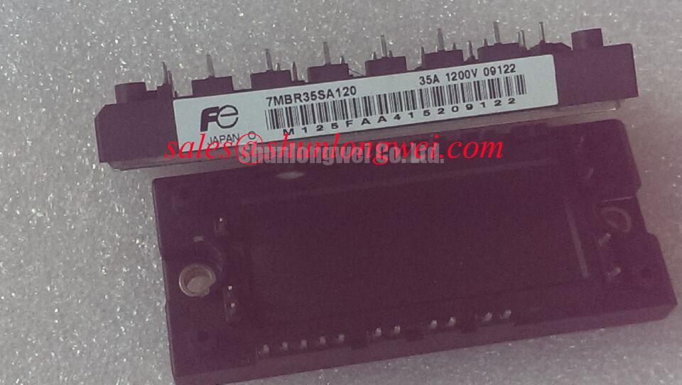
The module may be assessed alongside the 7MBR35VM120-50 when a maintenance team is comparing related Fuji Electric power-module references. This is a neutral comparison point, not a substitution instruction. Pin arrangement, internal topology, electrical ratings, and driver requirements must be checked against the original equipment documentation before any change is made.
Transient Dynamics & Electrical Design: Auxiliary Emitter Pinout Cold-Check on 7MBR35VW120-50
A cold check should begin by separating the main load-emitter terminal from any auxiliary or Kelvin-style emitter return shown in the applicable terminal drawing. These connections are not interchangeable in a fast gate-drive loop. The main emitter carries the load-current return, while an auxiliary emitter connection, when provided by the exact module configuration, is intended to give the driver a cleaner voltage reference. The correct pin identity must be taken from the matching Fuji Electric terminal documentation rather than inferred from physical position.
With the equipment isolated and the DC link fully discharged, trace the driver return from the gate resistor to its designated emitter reference. Check for unintended continuity through copper pours, mounting hardware, shields, or measurement equipment. A cold resistance check can identify an open connection, an unexpected short, or a misplaced link, but it cannot reproduce the voltage developed by load current during switching. If the gate waveform changes substantially when the motor current rises, use a differential probe to compare the driver reference with the module emitter at the terminals.
Ground bounce in the shared emitter path can appear as a false gate command or as an apparent reduction in gate voltage. The effect is especially important in a phase-angle-controlled power stage, where the current conduction interval changes with the command and the supply ripple, if that topology is used. For a servo actuator, line-frequency ripple smoothing and the DC-link control loop should be reviewed together with the gate-drive timing. The braking chopper must not be treated as an isolated accessory because its switching activity can couple into the same reference network.
RC snubbers are a Design Consideration for suppressing ringing across a switching node or braking device. Their value and placement should be selected from measured ringing frequency, voltage stress, switching loss, and resistor pulse capability. Do not apply a generic snubber value to this module without checking the complete commutation loop. A snubber that reduces overshoot can also increase turn-on or turn-off loss, so the thermal result must be checked at the intended duty cycle.
When a gate driver uses an optocoupler or digital isolator, assess common-mode transient immunity as part of the interface review. The isolation component must tolerate the measured switching-node movement without producing an unintended pulse at the gate input. Keep the isolated signal path away from the collector and braking-node copper, maintain a clear return strategy on the driver side, and verify propagation delay under the actual temperature and supply conditions. The module itself should not be described as independently compliant with an EMC standard; EMC performance belongs to the complete drive assembly.
For a front-end topology that includes a rectifier or auxiliary power stage, the 7MBR75VX120-51 can be reviewed as a related power-stage reference. Its presence in a system does not define the requirements of the 7MBR35VW120-50. The service engineer should confirm the DC-link charging sequence, braking threshold, phase current measurement method, and isolation architecture for the specific controller.
Maintenance Note: De-energize the drive and verify the DC-link discharge state before disconnecting any gate-drive cable or touching the module terminals.
Benchtop Waveform Tuning: Mitigating Stress via Pollution Degree 3 Creepage Distances on 7MBR35VW120-50
On the bench, inspect the high-voltage terminal area for dust films, moisture residue, carbon tracking, loose hardware, and contamination trapped between the module body and heatsink assembly. Pollution Degree 3 is a Design Consideration for industrial cabinets exposed to conductive dust or condensation; the required creepage and clearance are determined by the working voltage, insulation system, material group, overvoltage category, and applicable safety standard. The 1200.0 V rating of the 7MBR35VW120-50 does not by itself define the spacing required on a populated drive board.
An insulation audit may use an insulation test voltage permitted by the equipment safety procedure and the module documentation, with an acceptance criterion established by the applicable equipment standard or maintenance procedure. Treat this as an Engineering Recommendation for a maintenance test, not as an official product rating. Disconnect sensitive gate-drive, sensing, surge-protection, and auxiliary circuits before applying the test voltage. Record the test arrangement, duration, temperature, humidity, and the points connected to the instrument so that later readings remain comparable.
Where the construction uses an insulated ceramic substrate, inspect the isolation path for mechanical damage, solder splash, mounting distortion, and contamination around the terminal edges. Do not assume that a satisfactory cold resistance reading proves safe dynamic insulation. Recheck after the module is installed, the heatsink is secured, and the cable harness is routed in its final position. A change after assembly can reveal pressure, debris, or a clearance issue that was not present on the loose component.
The PCB interface should be reviewed using the established creepage and clearance rules applicable to the equipment. The FR-4 material reference is useful when assessing the board substrate, but it does not replace the insulation coordination required for the actual working voltage and pollution environment. Keep slots, cutouts, mounting hardware, and connector bodies in the same review because the shortest effective path may not follow the visible copper route.
Waveform tuning should proceed after the isolation and mechanical checks are complete. Probe the switching node with a suitable high-voltage differential probe, keep the probe loop compact, and compare the voltage overshoot during acceleration, steady motion, and regenerative braking. Observe whether the braking resistor absorbs energy smoothly or whether the DC link rises during deceleration. The RMS current method described in the RMS current reference can support conduction-loss evaluation, but the current waveform of the actual actuator must be used rather than a nominal motor-current label.
In service, clean the heatsink and confirm that airflow is not blocked by dust accumulation or cable routing. Inspect thermal-interface material for drying, pump-out, uneven contact, or contamination when the module is removed. Check terminal tightness using the equipment manufacturer’s specified procedure, then repeat the thermal survey under a representative load. A rising terminal or heatsink temperature should prompt a coordinated review of contact condition, current waveform, switching loss, airflow, and enclosure humidity rather than an immediate assumption of semiconductor failure.
For broader application context involving high-frequency induction-heating and power-switching principles, consult Power and Precision. The reference is a technical background resource; the integration limits for this Fuji Electric module must remain tied to its specified ratings and the verified behavior of the complete drive.