Content last revised on October 8, 2026
Infineon BSM15GD120DLC Replacement Checks and Product Overview
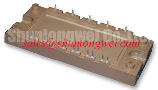
Before energizing a replacement assembly, isolate and discharge the DC link according to the equipment service procedure, inspect the module terminals for heat discoloration, and verify the cold resistance relationships against a known-good phase leg. The Infineon BSM15GD120DLC is an IGBT module specified at 1200 V and 15 A, with a Module package designation. These ratings do not establish unrestricted operating limits; actual operating limits depend on the datasheet conditions, switching frequency, thermal conditions, gate-drive behavior, and the completed equipment design.
| Manufacturer | Infineon |
| Part number | BSM15GD120DLC |
| Device category | IGBT Module |
| Rated voltage | 1200 V |
| Rated current | 15 A under the specified datasheet conditions |
| Package | Module |
For equipment repair, the part number should be checked against the original electrical schematic, terminal arrangement, gate-driver board, mechanical footprint, and thermal interface. A matching voltage and current label alone does not establish drop-in compatibility. Confirm the power terminals, auxiliary terminals, gate polarity, isolation arrangement, clamping method, and cooling interface before applying drive pulses.
Thermal Cycling Margins of Braking IGBTs under Repetitive Stop-Start Duty
In a precision stepper or BLDC servo actuator, deceleration energy can raise the DC-link voltage quickly when the motor changes from motion to braking. Depending on the equipment topology, the braking path may use a switching device integrated into a power assembly or an external braking IGBT, together with a ballast resistor selected by the system designer. This does not establish that the BSM15GD120DLC contains a dedicated braking switch. The 1200 V rating of the BSM15GD120DLC is an official device parameter, not a permission to operate continuously at that voltage. The actual peak must be checked during the fastest commanded stop, regeneration event, and fault recovery sequence.
Start the investigation at the machine terminals. With power removed and the DC link discharged according to the equipment service procedure, inspect the power connections for looseness, oxidation, carbon tracking, and uneven pressure. Measure the braking resistor separately from the semiconductor module, because a resistor that has drifted upward can increase DC-link overshoot while a damaged resistor can prevent energy absorption altogether. Record the DC-link waveform during controlled deceleration with a properly rated differential probe and compare it with the switching device voltage boundary.
Thermal cycling is governed by the energy absorbed per stop, stop frequency, junction-to-case thermal path, case temperature, heatsink condition, and the cooling system response. These values are system-dependent and are not supplied by the basic product data provided for this page. Designers should calculate the braking energy from the actual motor inertia, speed, load profile, and deceleration time, then determine the portion dissipated in the braking switch and validate the resulting junction temperature under the complete repetitive duty cycle.
Cold-start operation deserves a separate check. Grease viscosity, fan response, enclosure airflow, and temperature-sensor delay can change the first few braking events compared with a warm machine. When the actuator operates below ambient laboratory conditions, verify the control response time and DC-link rise during the first stop rather than relying only on a steady-state thermal test. Vibration and mechanical shock can also alter heatsink contact pressure or fatigue a heavy busbar, so the power path should be inspected after environmental testing.
⚠️ Field Alert: Do not reuse a heat-transfer interface that has been disturbed during replacement; clean both mating surfaces and follow the equipment manufacturer’s specified mounting method and torque instead of applying an assumed value.
For a neutral comparison during a service assessment, engineers may review the FF150R12ME3G alongside the installed device. It should not be treated as an automatic substitute; terminal layout, electrical characteristics, gate-drive requirements, thermal impedance, and protection settings require documented verification.
Isolated DC-DC Power Supply Sizing for High-Side Floating Gate Drivers
A high-side gate driver must maintain a stable floating supply while the phase node moves rapidly between switching states. Before replacing the power module, probe the driver supply at the gate-driver pins, not only at the isolated converter output. A supply that appears correct at no load may collapse during gate charging, produce excessive ripple, or lose regulation during repeated PWM operation.
The required insulation class and common-mode transient immunity are system-level design considerations. The frequently discussed targets of more than 5 kV isolation and more than 100 kV/µs CMTI must be confirmed from the selected DC-DC converter, isolator, PCB construction, and test method; they are not official ratings stated here for the BSM15GD120DLC. The system integrator should verify creepage, clearance, insulation coordination, transformer construction, and the complete gate-driver isolation barrier against the applicable equipment standard.
Gate-drive supply sizing should account for gate charge, switching frequency, driver quiescent current, pull-up and pull-down losses, bootstrap or isolated-converter behavior, and transient load current. The required sourcing and sinking peak current belongs to the driver and switching design, not to the module’s basic 1200 V and 15 A identification data. A bench supply test should include the actual gate resistor, driver output stage, isolated power path, and representative switching waveform.
External gate resistance is normally used to control the compromise between switching loss, voltage overshoot, electromagnetic disturbance, and cross-conduction risk. Begin with the resistance documented by the original equipment design when available. If that information is unavailable, select a conservative starting point for laboratory tuning and observe gate voltage, collector-emitter voltage, phase-node ringing, and device temperature. The final value must be established by measurement because stray inductance and driver output impedance vary between assemblies.
For a precision motion actuator, cold operation can expose marginal gate-drive supply behavior. Check the isolated converter during the first enable command, rapid direction reversal, and low-temperature PWM operation. If an auxiliary display or control panel uses PWM dimming, a 200 Hz to 1 kHz control range should be treated as a system timing consideration only; it is not a switching-frequency specification for this IGBT module. Confirm that display control activity cannot disturb the gate-driver supply or introduce timing jitter into the motor-control loop.
The FZ600R12KE4 may be evaluated as a separate upstream or complementary power-stage component when tracing a complete converter topology. Its presence in a related system does not establish electrical interchangeability with the BSM15GD120DLC.
Desaturation Detection and Two-Stage Soft Turn-Off Short-Circuit Protection
When a repaired drive trips immediately after enable, first separate a genuine load fault from a protection-circuit fault. Check the motor cable insulation, phase-to-phase resistance, phase-to-earth leakage according to the service procedure, gate waveform integrity, and the desaturation input with the power stage disabled. A short-circuit indication can also result from an incorrectly connected sense path, an unsuitable blanking network, driver supply instability, or excessive switching-node noise.
Desaturation protection measures an abnormal increase in the switching device’s collector-emitter voltage while a commanded gate pulse is present. The detection threshold, blanking interval, filter response, and comparator behavior are properties of the gate-driver circuit. A requested response time below 10 µs may be used as a design target for a particular protection architecture, but it is not an official short-circuit response specification supplied for this product. The total fault-clearing time, including detection and turn-off, must remain within the device’s documented short-circuit withstand conditions. Engineers should validate the complete protection chain with a controlled test method and the manufacturer’s safe operating guidance.
Two-stage soft turn-off is commonly considered when abruptly removing gate drive would create excessive inductive voltage overshoot. The first action reduces the gate discharge current or moves the device toward a controlled transition; the second action completes turn-off. The timing and gate levels must be designed around the actual driver, parasitic inductance, DC-link voltage, and load current. Avoid copying a protection delay from another module without checking the resulting collector-emitter waveform.
During troubleshooting, use a high-bandwidth differential measurement method suitable for the DC-link voltage and keep the probe loop physically short. Inspect the gate-emitter waveform at the module pins, because a clean signal at the driver board can become distorted by connector inductance, shared emitter impedance, or a damaged interface. If the fault appears only at elevated current, compare the turn-off transient with the DC-link voltage and verify that the clamp and snubber network remain within their intended operating range.
High-voltage spacing around the power loop and protection sense traces should follow the equipment insulation design. Keep noisy switching copper away from low-level desaturation and fault-reset signals, and verify that shield termination does not create an unintended current path through the gate-driver reference. The Field Engineer’s Handbook provides a practical reference point for structured testing and failure analysis.
For manufacturer information concerning power semiconductor technology and related intelligent power modules, consult Infineon Technologies and the Infineon CIPOS™ Mini IPM Series. These resources should be used to confirm the characteristics of the specific device family under evaluation rather than to infer unlisted parameters for this model.
Dynamic Gate Impedance Control for Robust Phase-Leg Dead-Time Operation
After a module replacement, confirm dead-time behavior with the motor disconnected or with a controlled low-energy test setup before returning the actuator to production. Observe both complementary gate signals at the module terminals and verify that neither command overlaps during enable, disable, direction reversal, or fault reset. A phase leg can experience shoot-through when high dv/dt couples through device capacitances, when the driver reference moves, or when a gate resistor or clamp connection has become intermittent.
Active Miller clamping can reduce unwanted gate movement during the opposite device’s switching transition, but its effectiveness depends on clamp placement, driver architecture, common-emitter impedance, and the voltage at which the clamp becomes active. A dedicated low-impedance return path should minimize parasitic loop inductance, while the final layout must be verified through measured gate and phase-node waveforms. The BSM15GD120DLC identification data provided here does not define an active Miller-clamp requirement.
Negative gate bias between approximately −5 V and −15 V is sometimes evaluated to improve off-state immunity in high-noise bridge designs. That range is a design consideration for the selected gate driver and semiconductor combination, not an official operating requirement for this module. Before applying negative bias, verify the device gate-emitter limits, driver isolation, power-up sequence, fault behavior, and the possibility of gate overstress during ringing.
Dead-time selection should account for turn-off delay, driver propagation mismatch, temperature, load current, diode recovery behavior, and the actual switching transition. Excessive dead time can increase conduction loss and distortion in a servo actuator, while insufficient dead time can create destructive current overlap. Tune it with current-limited testing and confirm operation at cold start, warm operation, rapid stop-start cycling, and the highest commanded acceleration.
When unexplained heating occurs, compare the two devices in the phase leg rather than assuming that the replacement module is defective. Check gate amplitude, plateau duration, turn-off tail behavior, DC-link ripple, phase-current symmetry, and mechanical pressure at the thermal interface. The 1200 V, 15 A, and Module specifications help identify the procurement item; safe performance depends on the complete gate drive, protection network, cooling path, and motion-control operating profile.