Content last revised on October 14, 2026
BSM75GB60DLC Operational Boundaries: Evaluating DC Bus Low Inductance and Laminated Busbar Limits
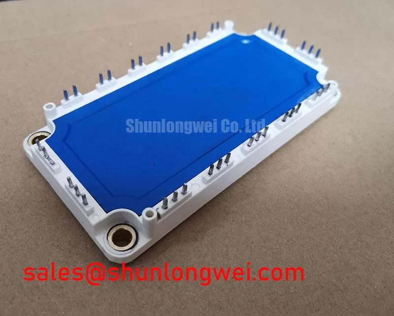
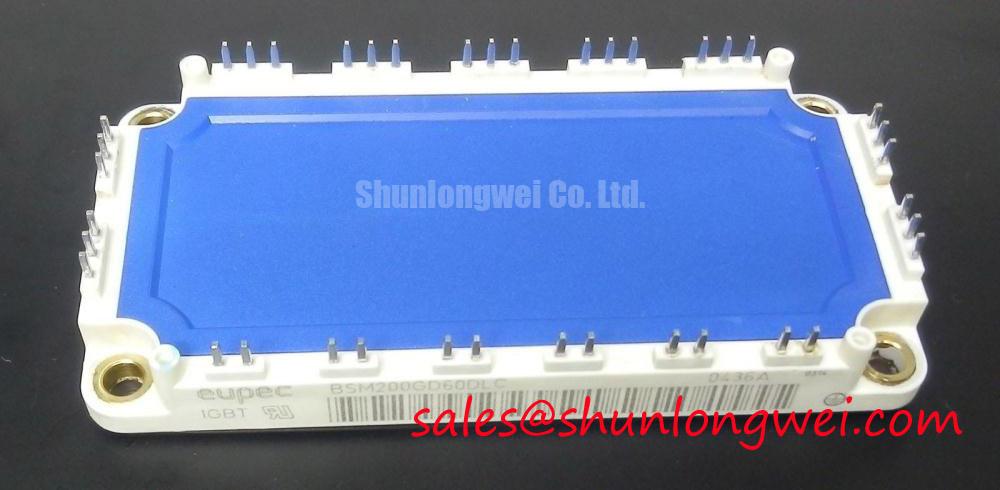
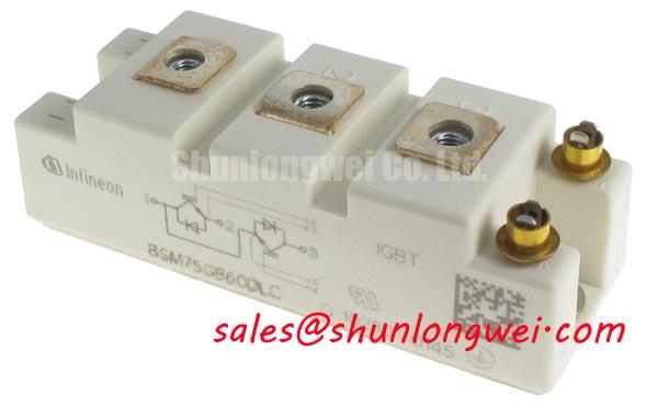
With the high voltage supply isolated, I first compare the replacement module’s marked terminals with the approved converter drawing, then inspect the DC bus interface for loose hardware, uneven contact, or contamination. The BSM75GB60DLC is an Infineon half-bridge IGBT module with a specified collector-emitter voltage rating of 600 V in the 75 A current class. These values establish the component classification, while the installed converter determines switching stress, thermal conditions, protection settings, and allowable transient margin. Allowable operating current depends on the datasheet conditions and the application’s cooling and duty cycle.
Turn off overshoot is strongly influenced by the commutation loop. In practical terms, the transient peak rises with DC bus voltage, stray loop inductance, and the rate of current change. The familiar relationship between these quantities is useful during waveform review: the inductive contribution is proportional to Lσ multiplied by di/dt and is added to the applied bus voltage. It should be treated as an engineering calculation rather than a factory specification for this module.
A laminated busbar can reduce the area enclosed by the forward and return current paths, but the result depends on the complete mechanical stack. I check the positive and negative layers for symmetry, confirm that the module terminals sit squarely against the intended copper interfaces, and examine whether capacitor connections are physically close to the switching loop. Long unpaired conductors, narrow necks in copper, and offset capacitor takeoffs can add inductive voltage even when the average bus voltage appears normal.
For a wind turbine full scale converter, the DC link should be reviewed as a complete energy path rather than as an isolated module connection. The rectifier or generator side, link capacitor bank, switching bridge, braking branch, and grid side each contribute to commutation behavior. A braking chopper and resistor bank may absorb regenerative energy, but their duty cycle and thermal capacity remain system determined. The BSM75GB60DLC rating does not by itself define the acceptable braking energy profile.
When measuring the switching node, use an appropriately rated differential or isolated probe arrangement suitable for the voltage, common mode voltage, and transient conditions, and keep the measurement loop compact. Compare the observed peak collector-emitter voltage with the module’s voltage rating and the converter’s documented transient limits; review the DC link voltage and protection threshold separately. Never connect an earth-referenced oscilloscope ground lead directly to a live switching node. If the peak changes when the probe arrangement changes, treat that result as a measurement setup issue until confirmed. A ringing waveform can also be associated with busbar geometry, capacitor placement, gate loop coupling, or diode recovery, so the waveform should be correlated with gate voltage and current rather than assigned to one cause.
Snubber selection belongs to the assembled converter. An RC network can reduce ringing by providing a controlled high frequency current path, but excessive capacitance increases switching loss and may alter commutation timing. Designers should select the network from measured overshoot, ringing frequency, pulse energy, and thermal results, then verify the result under the highest intended DC link and current conditions. The target loop inductance must be established by the system designer through layout analysis and switching tests, not presented as an unconditional property of the module.
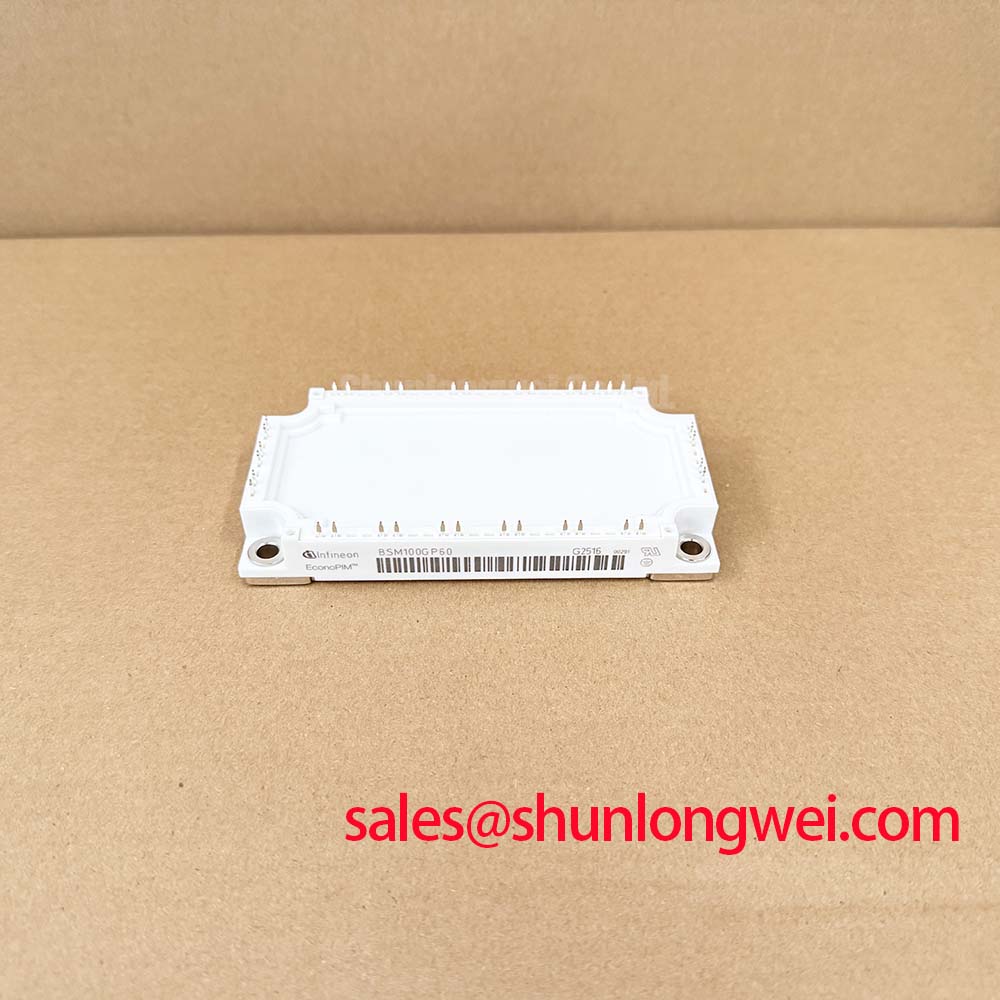
For a neutral comparison during service planning, engineers may review BSM100GD60DLC as a related Infineon module listing. That comparison does not establish interchangeability. Terminal arrangement, electrical characteristics, gate drive behavior, mechanical envelope, and thermal interface requirements must match the original converter design before any alternate part is considered.
Field Diagnostics and Commissioning: Gate Driver Auxiliary Power Sequencing in BSM75GB60DLC Topologies
Commissioning should keep the high voltage DC link disabled until the isolated gate driver supply, logic enable path, undervoltage lockout, and fault feedback have reached their intended states. I verify the driver output at the module interface with the power stage inactive, checking that the command signal is not floating during auxiliary supply startup. A negative turn off bias may be used by a particular driver design, but its value, timing, and suitability must come from the driver and module application documentation rather than from the BSM75GB60DLC current and voltage ratings.
Stable sequencing matters because a partially powered driver can produce an undefined gate condition. The commissioning record should capture auxiliary supply rise, reset release, fault clearance, enable transition, and the first controlled switching event. If the driver reports undervoltage lockout during a current transition, inspect supply impedance, local decoupling, isolation behavior, and common mode displacement before changing the gate resistor.
The thermal interface deserves the same discipline as the electrical interface. The baseplate and heatsink should be clean, flat within the mechanical limits specified by the assembly design, and free from particles that create local pressure points. Thermal interface material should be applied according to the material supplier’s process window and the module manufacturer’s mounting instructions. A thicker layer is not automatically safer; excess material can increase thermal resistance, while insufficient coverage can leave air pockets.
Mounting pressure should be applied progressively and evenly across the module. A cross pattern is a sensible mechanical practice when it agrees with the approved assembly procedure, but the final torque must be taken from the applicable mechanical documentation for the module, fastener, washer, and heatsink combination. After tightening, inspect the interface for rocking, corner lift, or displaced compound. These checks are more useful than treating a generic torque value as an official parameter for this specific product.
In a converter with several parallel current paths, static and dynamic sharing require separate attention. Positive temperature coefficient behavior can support current balancing in parallel semiconductor paths, yet it does not remove the need for matched gate drive paths, similar power loop geometry, and consistent thermal coupling. Designers should verify sharing at startup, rated operation, overload transition, and regenerative operation with current probes placed consistently in each path.
The upstream stage also affects the module’s operating environment. A system may include an active front end built around a module such as BSM35GD120DN2E3224, but that device should be evaluated as a separate element in the topology. Its voltage class, switching behavior, thermal path, and control timing must be coordinated with the DC link and gate driver rather than inferred from the BSM75GB60DLC designation.
Bench Tip: Keep the module and driver protected against ESD, record a cold state reference, and compare gate terminal readings with the known good channel before connecting the high voltage DC link.
Benchtop Waveform Tuning: Mitigating Stress Through Oscilloscope Verification
When a legacy drive board is adapted to a newer module, I begin waveform tuning with the gate command, gate to emitter voltage, collector to emitter voltage, and phase current on the same time base. The purpose is to see whether a change in external turn on or turn off resistance improves the switching transition without creating excessive ringing, delay, or thermal loss. The original gate driver output capability must be checked before selecting a resistor value.
Separate turn on and turn off paths can provide useful control over the compromise between switching loss and current slew rate. A lower turn on resistance may shorten the transition but increase di/dt, electromagnetic coupling, and commutation stress. A higher value may soften the edge while increasing dissipation. Turn off behavior should be evaluated for collector voltage overshoot, gate bounce, and any indication that the driver is being pulled outside its intended operating region.
The oscilloscope record should include several operating points rather than one visually clean pulse. Review light load, normal load, regenerative current, hot steady state, and the operating point that produces the highest observed voltage peak. The switching waveform should be compared with the DC link measurement and the driver fault timing. If a fault appears only after thermal soak, inspect the thermal interface, gate supply stability, and switching loss before attributing the event to the resistor alone.
Gate loop geometry is part of the tuning process. Keep the outgoing and returning gate paths paired, avoid routing them beside high current commutation conductors, and maintain the clearance required by the converter insulation design. Common emitter movement can make the measured gate voltage appear different from the driver reference. A differential measurement at the module terminals helps distinguish actual gate behavior from ground lead pickup.
Thermal validation should follow waveform changes because a smoother voltage trace may still increase average switching loss. Use the module’s applicable transient thermal impedance data and the converter’s pulse profile to estimate junction temperature behavior, then confirm the result through the approved thermal measurement method. The peak junction temperature margin is determined by the complete pulse sequence, case temperature, cooling system, and electrical duty cycle, not by the 75.0 A label alone.
Infineon’s power semiconductor information, including its OptiMOS and CoolMOS Power MOSFETs material, can provide useful background when comparing switching technologies at the system level. It should not be used to transfer MOSFET gate behavior or ratings directly to this IGBT module. Likewise, the Infineon EasyPACK product family is a separate product context and does not establish a substitute for BSM75GB60DLC.
Preventing Spurious Faults: Commutation Turn Off Voltage Suppression Guidelines
During a commutation event, the antiparallel diode and the opposing switch influence reverse recovery current, current slew rate, and voltage ringing. I review the phase current and switching voltage together, looking for a recovery event that coincides with gate disturbance, protection trips, or unexpected common mode movement. The peak reverse recovery current and its rate of change are determined by the diode, current level, temperature, bus layout, and switching conditions, so they must be measured in the assembled topology.
A snappy recovery event can excite the parasitic inductance of the power loop and produce a voltage spike that couples into the driver or control wiring. An RC snubber may reduce the resulting oscillation when its placement is close to the relevant commutation path. Its values should be selected from measured ringing behavior and pulse loss, with resistor heating and capacitor voltage stress included in the verification. A snubber placed far from the switching loop may have limited effect and can introduce another unintended current path.
Turn on gate resistance is another tuning variable. Increasing it can reduce the speed of the current transition and may lower ringing, while decreasing it can increase switching speed and associated electromagnetic coupling. The correct setting is the one that satisfies the converter’s switching loss, voltage stress, thermal, and fault response requirements together. It should be validated with the actual driver, busbar, diode path, and DC link rather than copied from an unrelated assembly.
For technical troubleshooting and broader topology context, engineers can consult the Industrial Applications reference while keeping the analysis specific to the installed converter. Offshore and onshore wind turbine converters may face long cable routes, changing generator conditions, and regenerative transitions, but enclosure, insulation, cooling, and EMC performance remain system responsibilities.
If a fault disappears when switching frequency or load is reduced, document the exact operating change and then separate electrical stress from thermal accumulation. Inspect gate supply behavior, current sensor timing, snubber temperature, busbar joints, and protection threshold timing. This approach avoids assigning a single cause to a complex commutation event and produces a repeatable record for engineering review.