Content last revised on October 16, 2026
Transient Dynamics and Electrical Design: Mechanical Stress Control for BSM75GD170DL
Check the main power terminal engagement and washer seating before applying switching voltage. On a high power module, a terminal connection that is mechanically uneven can transfer tightening or vibration forces into the copper current path. The result may appear later as intermittent heating, unstable switching, or a change in connection resistance during thermal cycling.
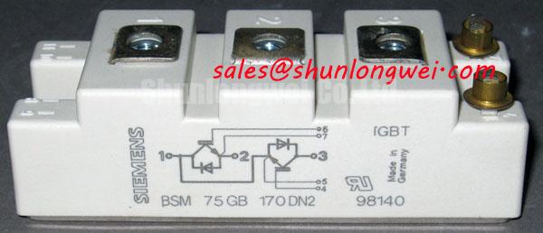
The BSM75GD170DL is an Infineon IGBT module with an official voltage rating of 1700.0 V and a rated collector current of 75.0 A under the specified datasheet conditions. These are device ratings, not a complete traction inverter operating prescription. The surrounding DC link, switching frequency, cooling system, gate driver, protection circuit, and mechanical assembly determine the usable operating envelope.
For incoming inspection, compare the terminal threads, washers, busbar contact faces, and mounting surface against a known good assembly. Look for tilted washers, damaged threads, uneven contact marks, or a busbar that has to be forced into alignment. The busbar should meet the terminal naturally, without acting as a lever when the fastener is tightened. This is particularly important in traction inverter cabinets exposed to vibration and repeated temperature changes.
Design Consideration: Keep the high current path short, mechanically supported, and separated from sensitive gate wiring. The power terminals should not carry the mechanical load of an unsupported busbar. When replacing a module, designers should verify the original fastening method, washer arrangement, conductor clearance, creepage requirements, and thermal interface condition against the equipment documentation.
During a fault investigation, record whether heating is concentrated at the module terminal, busbar joint, or cable transition. A thermal image can help locate the area of interest, while a cold resistance comparison between equivalent current paths can reveal an assembly inconsistency. Because contact resistance readings are strongly affected by probe force and measurement current, use the same instrument setup for the replacement comparison.
For systems with multiple power switching stages, a separate stage may use a device such as FZ1200R17KF6-B2. That reference is a system level association rather than a statement that the two products are automatically interchangeable. Voltage class, current path, gate drive arrangement, cooling, and mechanical interfaces must be assessed separately.
⚡ Safety Interlock Note: Isolate and discharge the DC link before loosening terminals or connecting test equipment, and verify the absence of hazardous voltage with an appropriately rated instrument.
Transient Dynamics and Electrical Design: Fault Clearing for BSM75GD170DL
Fault clearing should be designed around the complete power loop rather than the IGBT module alone. A short circuit or severe commutation event can produce rapid current change, and the stray inductance of busbars, laminated conductors, terminals, and capacitor connections can convert that current change into an overvoltage at the switching device.
For type I and type II short circuit protection, the gate driver should identify abnormal collector or desaturation behavior quickly and then apply a controlled turn off. A two stage soft turn off is a common Design Consideration: the first stage limits the rate of current interruption, while the final stage brings the gate to its defined off state. The actual detection delay, blanking interval, gate current, and clamp behavior must be established by the driver design and validated against the module datasheet limits.
The protection loop should be physically compact. Place the DC link film capacitor close to the switching current path, keep the forward and return conductors closely coupled, and avoid routing the fault detection signal alongside a high di/dt conductor. A snubber capacitor can be useful when switching tests show excessive ringing, but its value, voltage rating, pulse current capability, and placement are system determined.
When a switching waveform shows an unexpected collector voltage spike, inspect the complete commutation loop before changing the gate resistor. Check capacitor mounting, busbar overlap, terminal contact, probe ground inductance, and the physical distance between the module and the DC link capacitor. An incorrectly connected oscilloscope probe can create a false overshoot or conceal the real peak.
The specified 1700.0 V rating identifies the voltage class of the BSM75GD170DL. It does not by itself establish the permitted DC link voltage during switching transients. Engineers should measure the actual peak voltage at the module terminals under the intended load, temperature, gate timing, and fault conditions, then compare that result with the applicable manufacturer limits and the equipment protection requirements.
BSM75GD170DL Circuit Protection and Reliability: Gate Drive Loop Geometry
Separate the gate drive return from the high current emitter path wherever the module interface and driver design provide distinct return points. Shared copper can introduce common emitter impedance, allowing load current voltage drop to appear in the gate loop. That feedback may contribute to gate oscillation, uneven parallel switching, or an apparent change in turn off behavior.
This separation is a Design Consideration, not an unverified statement about the internal construction of this specific module. The integrator should follow the terminal definition and recommended circuit arrangement in the applicable Infineon documentation. If the installed assembly does not expose an auxiliary emitter connection, the return strategy must be evaluated from the actual terminal arrangement rather than assumed from another module family.
At the bench, connect the driver with the shortest practical gate loop and keep the gate path away from the collector and main emitter conductors. Confirm gate voltage directly at the module interface using a measurement method suitable for fast switching. Compare the rising and falling waveforms at low energy first, then repeat the observation under representative current and temperature conditions.
Miller charge associated with the collector to gate capacitance can couple a collector voltage transition into the gate circuit. An active Miller clamp may reduce unwanted gate rise during a high dv/dt event, but its threshold, response, wiring, and driver supply behavior are part of the gate driver design. Do not treat an active Miller clamp as a substitute for correct layout, adequate dead time, or a validated short circuit response.
Dead time should prevent simultaneous conduction in complementary devices, while excessive dead time can increase freewheel conduction losses. The correct interval depends on the switching devices, driver propagation delay, temperature, load current, and modulation strategy. Tune it from measured gate and collector waveforms rather than copying a value from an unrelated inverter.
When comparing possible parts for a repair, the BSM75GP120 may be reviewed as a separate product reference. Its voltage class, current capability, internal circuit arrangement, terminal layout, and thermal behavior must be compared with the original application before any substitution is considered. A similar part number or package description does not establish drop in compatibility.
Benchtop Waveform Tuning: Thermal Transient Evaluation for BSM75GD170DL
Evaluate pulsed overload by correlating the electrical waveform with the thermal path from junction to case and from case to heatsink. The purpose of a transient thermal model is to estimate how quickly a short power pulse can raise junction temperature before the case temperature instrument shows the change.
A multi resistance capacitance model can represent the transient junction to case response when the relevant manufacturer thermal impedance data are available. In practical testing, determine the device power loss profile and pulse energy from the measured voltage and current waveforms, use the loss profile with the appropriate transient thermal impedance data, and compare the estimated junction temperature with the permitted operating boundary. The model must use the pulse duration and duty cycle of the real event; a single steady state thermal resistance is not sufficient for every overload condition.
For a bidirectional DC to DC battery charger or traction inverter service test, log the switching waveform, case temperature, heatsink temperature, coolant or airflow condition, and repetition pattern together. Repeated charge and discharge operation can produce thermal cycling even when the average electrical power appears acceptable. The relevant question is not only whether the case feels stable, but whether the junction temperature repeatedly approaches a limit during the switching sequence.
Mounting flatness, thermal compound coverage, clamping uniformity, and heatsink cleanliness influence the case to heatsink path. Verify that the module base sits evenly and that the interface material is applied according to the equipment manufacturer’s assembly procedure. If the case temperature rises unusually fast, compare the mechanical installation with a known good assembly before changing the control parameters.
Waveform tuning should begin with conservative test energy and a calibrated differential voltage probe and current probe. Observe turn on, turn off, reverse recovery interaction, gate plateau behavior, and any ringing that coincides with a thermal rise. The measured collector voltage should be assessed at the module terminals, not only at a remote busbar point.
For broader application guidance on switching layout, protection coordination, thermal assessment, and power semiconductor selection, consult the Power Electronics Masterclass. Device family references such as Infineon PrimePACK™ and Infineon CIPOS™ Nano describe other Infineon product platforms and should not be interpreted as specifications for the BSM75GD170DL.