Content last revised on September 12, 2026
FZ1200R17KF6B2 Installation and Official Specifications
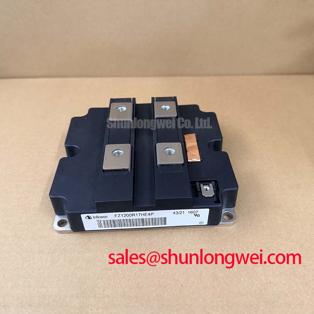
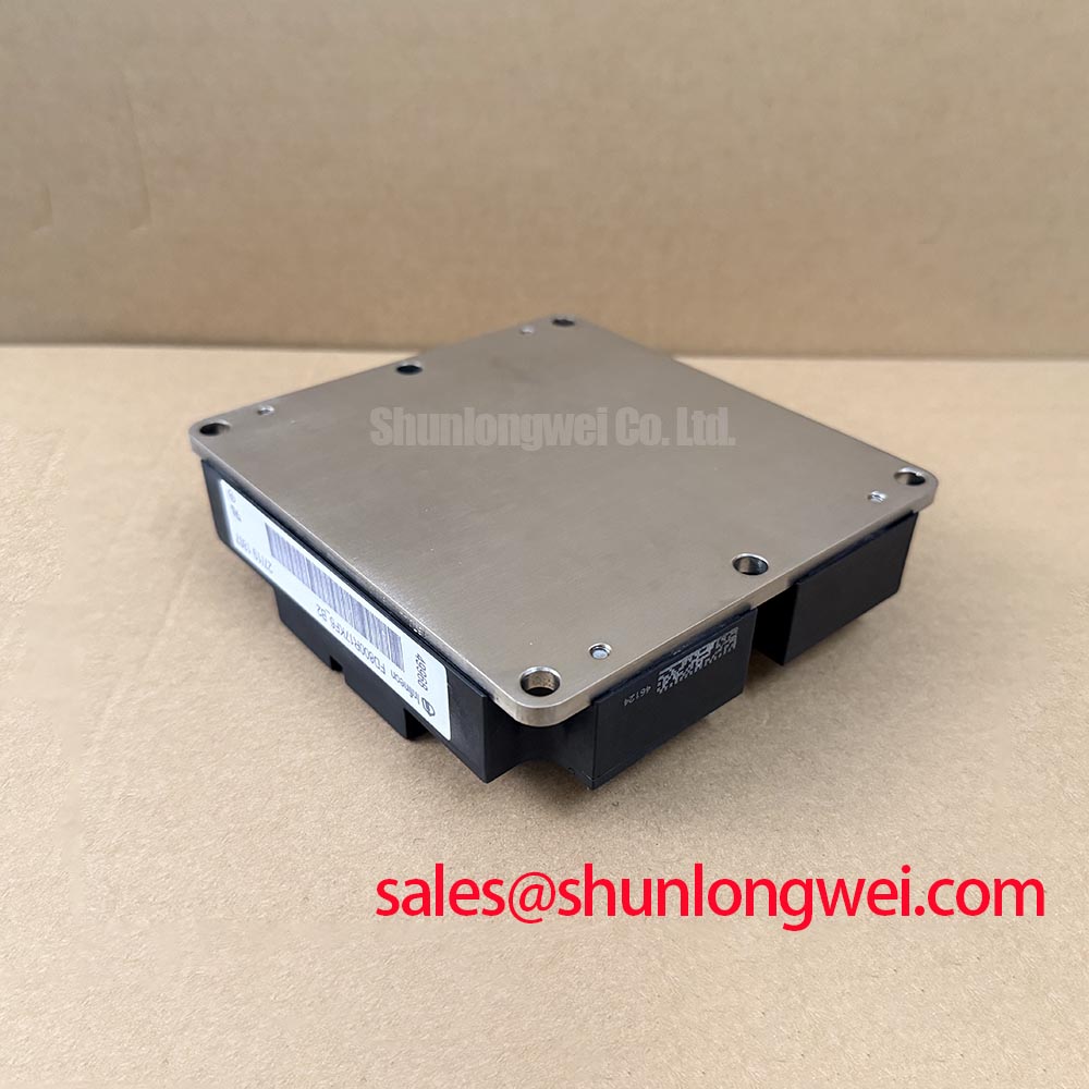
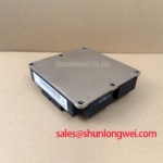
With the converter isolated and discharged, first verify the power terminal arrangement, mounting face condition, and nameplate rating against the service documentation before fitting FZ1200R17KF6B2. This Infineon single-switch IGBT module is officially rated at 1700 V collector-emitter voltage and 1200 A continuous collector current. Its official maximum power dissipation is 9.6 kW, maximum junction temperature is 150°C, and the module uses screw terminals with an IHM baseplate.
| Official Specification | Value |
|---|---|
| Manufacturer | Infineon |
| Collector-Emitter Voltage | 1700 V |
| Continuous Collector Current | 1200 A |
| Maximum Power Dissipation | 9.6 kW |
| Maximum Junction Temperature | 150°C |
| Configuration | Single-switch module |
| Mounting Technology | Screw terminal and IHM baseplate |
Assembly Integrity & Layout Architecture: Planar Symmetrical Busbar Geometry for FZ1200R17KF6B2
Before energizing a repaired power stack, inspect the IHM baseplate contact surface and the heatsink for old interface residue, corrosion, burrs, or uneven contact marks. These findings do not establish a module defect by themselves, but they can affect heat transfer and should be addressed before a replacement unit is commissioned. The 9.6 kW maximum power dissipation and 150°C maximum junction temperature are official limiting specifications, not operating targets. Actual thermal performance remains dependent on the heatsink, interface material, airflow, coolant condition, switching duty, and measured load profile.
Design Consideration: a symmetrical planar busbar arrangement reduces the area enclosed by the DC link commutation loop. During turn-off, peak collector-emitter voltage is influenced by DC link voltage plus the product of stray inductance and current change rate. The system engineer should minimize parasitic loop inductance to suppress inductive overshoot, then verify the actual peak voltage at the module terminals during switching tests. Snubber capacitor selection, placement, and energy capability must be validated against the converter operating waveform rather than copied from another power stack.
Keep positive and negative DC conductors physically paired where practical, avoid unnecessary conductor length between the DC link capacitor and power terminals, and inspect each busbar for flat seating. A bowed conductor can introduce uneven clamping force and intermittent contact resistance. For planned material substitution during a repair, the FF45017ME4 can be reviewed as a separate device option, but voltage class, current requirement, package geometry, driver interface, thermal path, and protection settings must be compared with the original system documentation before any engineering decision.
⚠️ Maintenance Note: Monitor terminal and heatsink contact temperature during service checks, and clean blocked cooling passages before interpreting elevated temperature as a semiconductor fault.
Field Diagnostics & Commissioning: PCB Gate Loop Layout Symmetry in FZ1200R17KF6B2 Topologies
For a module replacement, confirm every gate drive and power connection from the equipment schematic rather than relying on cable length, terminal position, or a prior installer’s markings. Check that the gate drive return path follows the intended reference connection and is not forced to share a high-current power return route. Design Consideration: shared inductance in the gate return path can convert rapid load current changes into unwanted gate voltage disturbance. The result may be ringing, unstable switching behavior, or protection events, but these symptoms require oscilloscope verification at the relevant gate and power reference points before assigning a cause.
Inspect insulation spacing around the gate driver PCB, busbar edges, fasteners, and measurement leads. Clearance and creepage requirements are determined by the complete converter voltage, pollution environment, insulation system, enclosure, and applicable equipment standard. They cannot be inferred from the 1700 V module rating alone. During commissioning, compare the observed switching waveforms with a known good channel or validated production waveform where available, while observing the equipment’s approved measurement and safety procedure.
Vibration can loosen hardware and alter the contact quality of a screw-terminal power path. Recheck fastener condition after initial thermal cycling and during scheduled preventive maintenance. This is a general maintenance practice, not an official torque specification for this module. Where the power stage works alongside rectifier or complementary converter hardware, the FZ3600R12HP4 may be examined as a separate power module reference; its electrical role and ratings must be evaluated within the full topology.
Field Diagnostics & Commissioning: Insulation Barrier Integrity in FZ1200R17KF6B2 Topologies
Do not assign a reinforced isolation rating or common-mode transient immunity value to FZ1200R17KF6B2 unless it is documented in the applicable Infineon module and driver documentation. The supplied official product data identifies a single-switch module with screw-terminal and IHM-baseplate mounting, but does not establish a complete isolated gate-drive barrier specification. Isolation responsibility is shared across the driver, PCB, connectors, cabling, enclosure, and the final converter construction.
When a drive produces unexplained gate activity, begin with objective checks: inspect the gate-driver supply stability, verify control-reference continuity, examine wiring routing, and capture switching behavior with suitable isolated measurement equipment. Common-mode disturbance can couple into poorly controlled signal paths, yet it should not be treated as the sole explanation for an abnormal pulse. Moisture, contamination, damaged cable insulation, degraded conformal protection, or a wiring error can create similar field symptoms.
For engineers comparing driver and adjacent switching technologies, Infineon’s CIPOS™ Nano IPM information provides context on integrated power module families, while its OptiMOS™ and CoolMOS™ MOSFET portfolio describes separate MOSFET technologies. Neither source should be used to transfer electrical, isolation, or switching specifications to this IGBT module.
Design Consideration: in cold industrial environments, inspect the enclosure for condensation paths before restart. Dry the affected equipment according to site procedure and verify insulation condition using the equipment manufacturer’s approved test method.
Transient Dynamics & Electrical Design: Long Motor Lead Reflected Wave Voltage on FZ1200R17KF6B2
Long motor cables can behave as transmission paths rather than simple conductors. Impedance mismatch between the inverter output, cable, and motor winding can produce reflected voltage at the motor terminals. Depending on cable construction, length, switching waveform, motor impedance, and filter arrangement, the observed motor terminal waveform can differ substantially from the waveform measured at the inverter. A voltage probe at one location should therefore not be assumed to represent the other.
When investigating insulation stress or recurring drive trips, record voltage at appropriate converter and motor points using a measurement method suitable for the installation. Compare cable routing, shielding termination, output reactor condition, and filter connections with the approved design. Designers should evaluate output filters and chokes where the measured waveform and motor insulation requirements justify them; component values and filter topology are system determined and must be validated across the intended speed, load, and temperature range.
The 1700 V collector-emitter rating defines an official module voltage boundary, while actual DC link level, transient amplitude, protection coordination, and motor lead behavior belong to the completed converter design. For broader background on how wide-bandgap devices introduce different switching tradeoffs in power conversion, see the Wide Bandgap Revolution technical discussion. It is a technology reference and does not alter the specified ratings or integration requirements of FZ1200R17KF6B2.