Content last revised on October 2, 2026
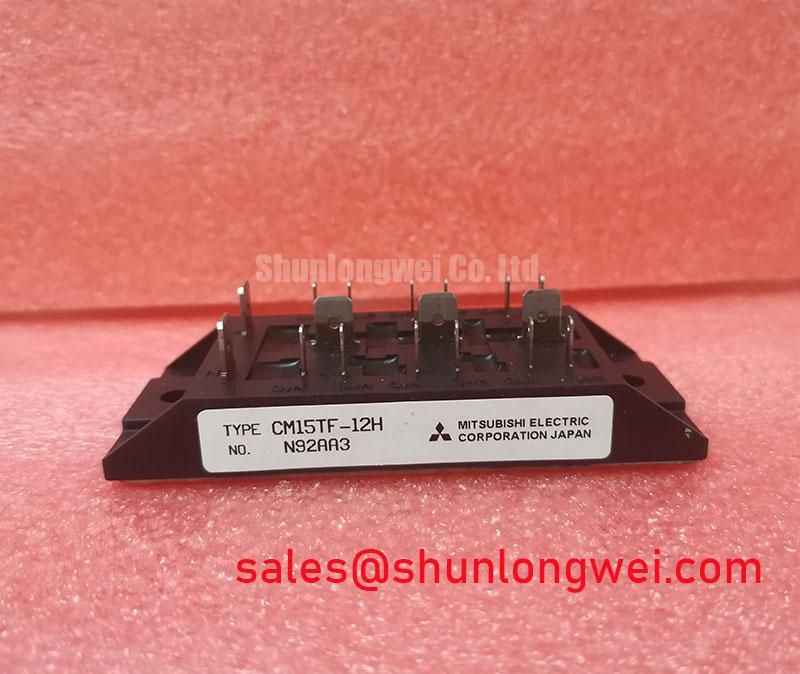
CM15TF-12 Thermal-Electrical Optimization: Thermal Time Constants and Peak Junction Practical Tuning
For a compact industrial inverter or high-speed CNC spindle drive, thermal verification should begin with the complete heat path rather than the semiconductor alone. Inspect the heatsink contact area, remove dust from the cooling path, and confirm that the fan or forced-air system is operating as intended. The CM15TF-12 carries an official current rating of 15.0 A, but the usable operating point in an installed drive depends on switching conditions, conduction duty, ambient temperature, cooling resistance, overload duration, and the actual waveform applied to the module.
A thermal transient model is useful when the load is pulsed. The case temperature does not immediately follow every current change; the heatsink, mounting interface, and semiconductor junction respond at different time constants. Designers should therefore evaluate the complete thermal impedance using the manufacturer’s published data where available, then compare the calculated junction temperature with the permitted operating boundary. A calculation based only on average motor current can miss short overload pulses, braking events, or repeated acceleration cycles that produce a higher junction temperature.
When no reliable thermal history is available, maintenance personnel can establish a baseline by recording heatsink temperature, ambient temperature, output current, switching state, and enclosure airflow during a known production cycle. Repeat the measurement after cleaning the heatsink and after inspecting the thermal interface. A gradual rise in contact temperature may justify checking mounting flatness, interface compound condition, fan performance, or blocked ventilation. It should not be assigned to the IGBT module without comparing the electrical waveform and cooling conditions.
The mounting interface also affects electrical reliability. Keep the power path mechanically stable, avoid twisting the module terminals during busbar installation, and ensure that the heatsink is not distorted by uneven fastener loading. The precise fastener method and torque should follow the applicable mechanical documentation rather than a generic value. ⚠️ Maintenance Note: Monitor contact temperature and clean the heatsink and airflow path at a planned maintenance interval, especially where conductive dust or condensation can enter the enclosure.
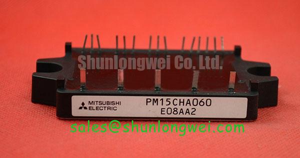
For a replacement assessment, the CM100DY-12E may be reviewed as a separate Mitsubishi Electric module in a side-by-side engineering comparison, but voltage, current, circuit topology, terminal arrangement, thermal data, and mechanical fit must be verified before considering any substitution. Similar package appearance does not establish electrical interchangeability.
Benchtop Waveform Tuning: Mitigating Stress via Thermal Feedback on CM15TF-12
Bench testing should reproduce the actual gate-drive reference, emitter return path, DC-link behavior, and load current direction used in the equipment. Measure the gate-to-emitter waveform at the module terminals with a suitable differential probe and keep the probe loop short. A controller-side gate signal may look clean while the module terminal waveform contains ringing caused by common-mode movement, stray inductance, or an unsuitable return path.
The positive temperature behavior often associated with the saturation voltage of IGBT structures can support current sharing under certain steady-state parallel arrangements, but it does not remove the need for symmetrical power and gate-loop construction. Dynamic sharing is strongly affected by gate resistance, driver output impedance, propagation delay, emitter inductance, device temperature, and layout symmetry. These conditions should be tested at the intended current and switching rate rather than inferred from a cold, low-current bench measurement.
Gate turn-off requires particular attention in a noisy inverter. A negative turn-off bias may be considered where the driver, isolation system, and device documentation support it, but the correct value is system-determined. Designers should verify the gate-emitter absolute limits, driver supply sequence, protection behavior, and the effect of common-mode ground bounce before applying any negative bias. A gate clamp can also be evaluated when overshoot remains after the physical loop has been improved.
High-side driver arrangements that use a bootstrap supply need a complete charge-balance review. The bootstrap capacitor must provide the required gate charge for the switching event while also supplying driver quiescent current, leakage, charging losses, and any level-shifter demand during the high-side on-time. The selection should be checked over the intended duty cycle, switching frequency, temperature range, and startup sequence. The bootstrap diode’s reverse-recovery behavior can disturb the driver supply and create a misleading gate waveform, so its dynamic behavior should be assessed with the driver and layout rather than selected independently.
For field troubleshooting, compare the suspect phase with a known-good phase at the module gate and power terminals. Look for unequal turn-on or turn-off delay, abnormal ringing, missing dead time, and a gate waveform that changes substantially with cable position or enclosure bonding. These observations may indicate a layout, driver, grounding, or measurement problem; they do not by themselves prove internal module damage. Record the oscilloscope bandwidth, probe arrangement, DC-link condition, and load state so that repeated measurements remain comparable.
CM15TF-12 Thermal-Electrical Optimization: Reinforced Insulation Barrier Integrity and Practical Tuning
Isolation must be evaluated as part of the complete power assembly. The CM15TF-12 product data supplied here confirms the voltage and current ratings, but it does not establish a specific reinforced isolation test voltage, common-mode transient immunity value, safety certification, or creepage and clearance requirement. Those values must be taken from the applicable manufacturer documentation and the equipment safety standard governing the finished inverter or spindle drive.
During maintenance, inspect insulation barriers, terminal spacers, busbar supports, cable jackets, and areas where dust or moisture can form a conductive path. High humidity and repeated temperature cycling can produce condensation even when the enclosure appears closed. The appropriate prevention method may include enclosure heating, controlled ventilation, drainage, conformal protection of suitable control assemblies, or improved sealing, but the final approach depends on the equipment environment and the responsible safety design.
Common-mode transients can couple from the power circuit into the gate-drive reference through parasitic capacitance and the mechanical structure. A practical design consideration is to keep high-current commutation paths physically separate from sensitive control returns, use a deliberate reference connection, and minimize the area of the gate-drive loop. The system engineer should verify the resulting gate-emitter waveform during the fastest intended switching transition and under the highest relevant DC-link condition.
When a drive shows intermittent triggering, nuisance protection trips, or unexplained phase imbalance, inspect the isolation power supply, gate-driver return, shield termination, and cable routing before replacing the module. Use a controlled low-energy test state where possible, then compare control-side and module-side signals. Insulation resistance testing, withstand testing, and any production safety test must follow the equipment procedure and the voltage limits specified for the actual assembly. A general component-page statement cannot replace that qualification.
The technical principles of gate-loop control, thermal management, bus structure, and switching stress can be reviewed in the IGBT Design & Integration guide. For a system that includes an upstream rectifier, the CM300DXDX1-24A may be evaluated as a separate complementary-stage device. Its ratings and topology must be checked independently from the CM15TF-12.
CM15TF-12 Thermal-Electrical Optimization: DC-Link Capacitance Bank Layout and Low-ES Practical Tuning
The DC-link layout determines how much switching stress reaches the module. During turn-off, stray inductance and current-change rate can create a voltage overshoot above the nominal DC-link level. The familiar relationship between overshoot, stray inductance, and current slew rate is useful as an engineering calculation, but the resulting peak must be verified with a properly connected high-voltage differential probe at the module terminals. A measurement taken far away at the capacitor bank can hide the local peak experienced by the switching device.
Place the high-frequency portion of the DC-link capacitance close to the power commutation loop, with short and broad connections between the capacitor, module, and return path. Symmetrical busbar geometry can reduce unequal current sharing between phases and limit magnetic coupling into gate-drive wiring. The required capacitance, equivalent series resistance, ripple-current capability, and physical arrangement are determined by the DC-link voltage, load profile, switching pattern, cable inductance, braking energy, and enclosure temperature.
Snubber selection should follow measured switching behavior. A snubber that is too small may provide little damping, while an unsuitable capacitor or resistor can add loss and increase thermal loading. Designers should first identify the ringing frequency and peak voltage with a repeatable probing method, then evaluate a damping network against the module’s voltage boundary and the drive’s efficiency target. The design should be validated during startup, acceleration, deceleration, regeneration, and fault interruption rather than only at steady-state load.
Capacitor banks also require mechanical and service attention. Check terminal tightness according to the equipment manufacturer’s procedure, inspect for swelling or leakage, and look for discoloration around busbar joints. An apparently sound capacitor can still exhibit changed electrical behavior, so capacitance, equivalent series resistance, ripple-current condition, and DC-link ripple should be assessed using suitable instruments when the maintenance process permits.
When the CM15TF-12 is evaluated for a compact inverter or CNC spindle drive, the final review should correlate four measurements: module terminal voltage, phase current, gate-emitter voltage, and heatsink temperature. If one phase behaves differently, compare its wiring length, gate-driver reference, sensor calibration, busbar pressure, and cooling contact before drawing a component-level conclusion. The module’s official identification for this page remains 600.0 V, 15.0 A, and Module package; all application limits must be confirmed against the original equipment design and applicable Mitsubishi Electric documentation.