



Content last revised on September 20, 2026
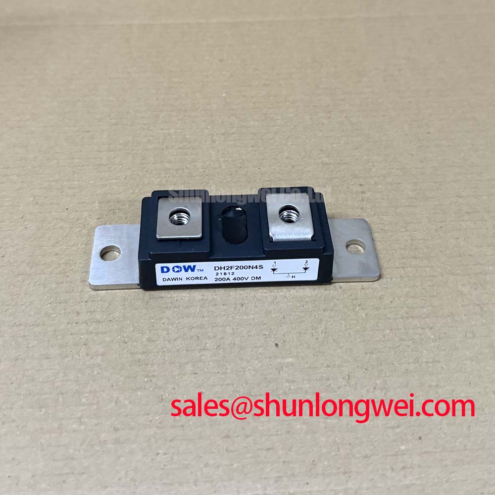
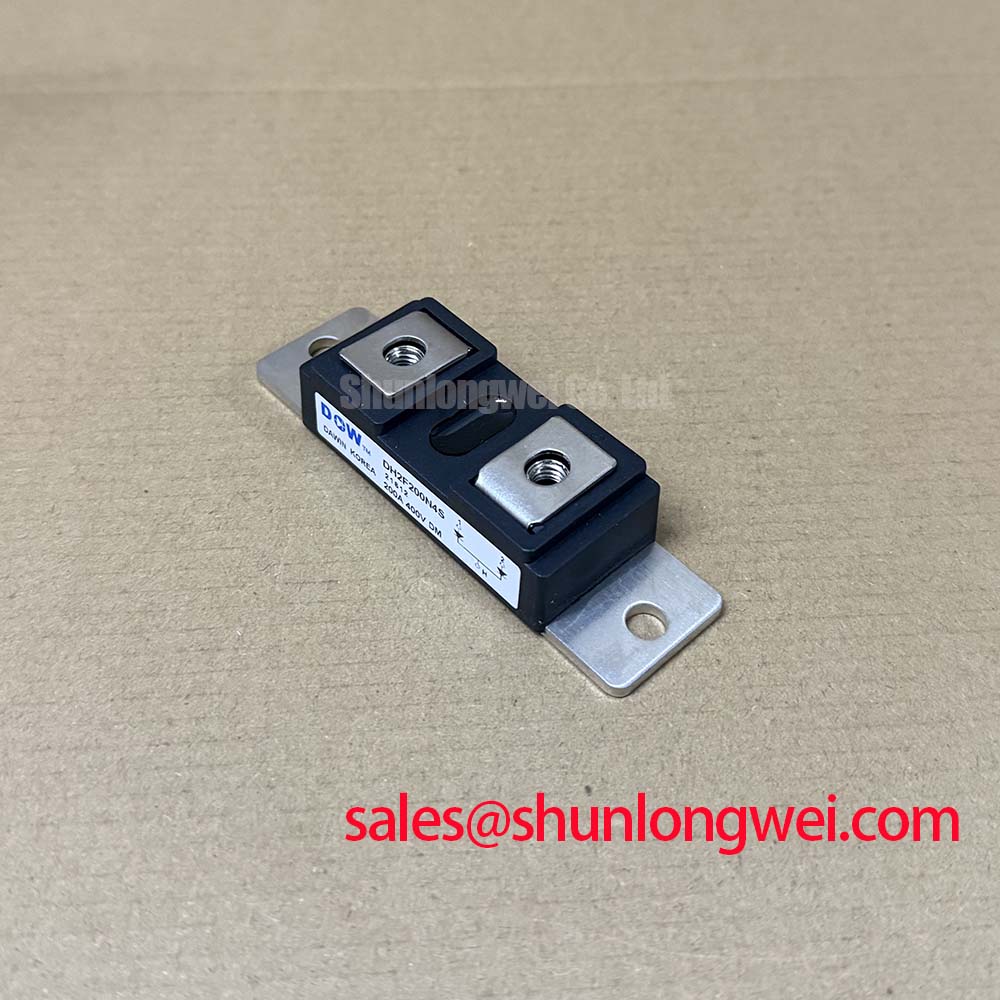
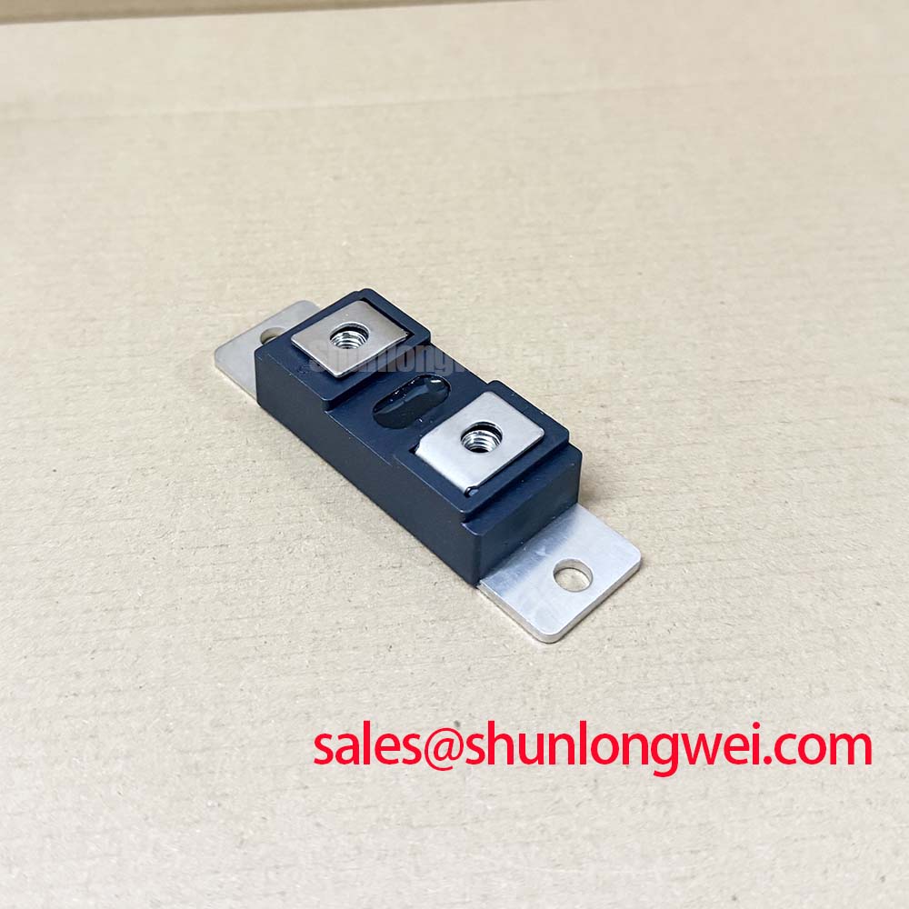
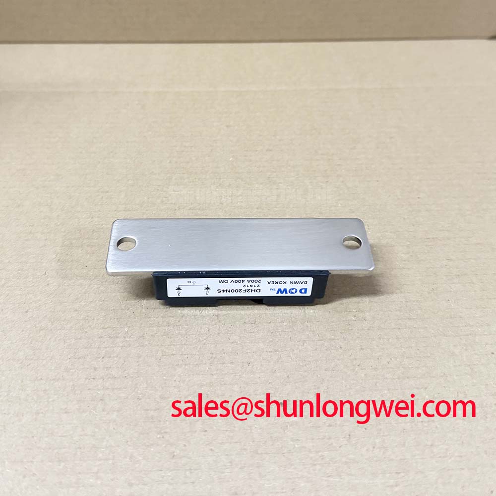
Before energizing a replacement, verify the DH2F200N4S nameplate, inspect the case and terminals, and confirm the installation’s voltage and current boundaries against the original circuit documentation. SanRex (Sansha Electric) specifies this IGBT and diode module for a 400 V collector-emitter voltage, with a 200 A continuous collector current at Tc = 80°C. These values define the component-level reference point; the complete converter still requires system-level validation of switching stress, cooling, surge exposure, and protection coordination.
| Parameter | Official Factory Specification |
|---|---|
| Collector-emitter voltage | VCES: 400 V |
| Gate-emitter voltage | VGES: ±20 V |
| Continuous collector current | IC: 200 A at Tc = 80°C |
| Pulsed collector current | ICM: 400 A |
| Diode continuous forward current | IF: 200 A at Tc = 80°C |
| Maximum power dissipation | PC: 780 W |
| Collector-emitter saturation voltage | 2.1 V typical, 2.7 V maximum at IC = 200 A and VGE = 15 V |
| Gate-emitter threshold voltage | 5.0 V minimum, 6.5 V typical, 8.0 V maximum at IC = 200 mA and VCE = 10 V |
| Turn-on energy | 2.5 mJ typical at IC = 200 A, VCC = 300 V, Tj = 125°C |
| Turn-off energy | 1.7 mJ typical; test conditions are not stated in the supplied data |
| Diode forward voltage | 1.7 V typical, 2.2 V maximum at IF = 200 A and VGE = 0 V |
DH2F200N4S Thermal-Electrical Optimization: Minimizing Commutation Turn-Off Voltage — Practical Tuning
When commissioning the commutation path, measure the actual switching waveform at the module terminals rather than estimating performance from the nominal current rating. The factory data gives a typical turn-off energy of 1.7 mJ, while the diode forward-voltage specification is 1.7 V typical and 2.2 V maximum at 200 A with zero gate-emitter voltage. The available factory data does not state diode reverse-recovery peak current, reverse-recovery time, or a soft-recovery factor, so these values should be obtained from the applicable technical documentation or characterized on the finished converter.
A practical design consideration is to keep the commutation loop compact and physically symmetrical, then verify voltage overshoot and ringing with a properly rated differential probe. The measured peak should be assessed against the 400 V VCES rating and the switching conditions used by the equipment. Gate-drive return paths, power-terminal geometry, busbar spacing, and snubber placement can influence the observed waveform; the system designer should confirm the result during representative double-pulse or operating tests.
For medium-frequency induction melting and metal hardening power supplies, the module may be evaluated in the inverter or controlled rectification section, subject to the topology and the original service documentation. A related device such as FRS200CA100 can be cross-referenced during maintenance planning, but pin arrangement, voltage class, current conditions, thermal interface, and dynamic behavior must be verified before any substitution.
Field Diagnostics & Commissioning: Baseplate Thermal Resistance in DH2F200N4S Topologies
Thermal commissioning should begin with a clean mechanical interface, a flat heatsink surface, and an even clamping sequence. The specified maximum power dissipation is 780 W, but this is not a complete heatsink design value. The usable operating point depends on case temperature, junction temperature limits, switching frequency, duty cycle, ambient conditions, thermal interface quality, and airflow or coolant performance. The original datasheet should be consulted for the module’s thermal resistance values and permitted mounting method where those details are required.
Inspect the baseplate contact pattern after installation and confirm that the heatsink does not distort the module body. Thermal compound should be applied as a controlled interface layer according to the compound manufacturer’s process guidance, without contaminating insulated surfaces or terminal hardware. During a loaded test, compare temperatures across the mounting area and examine whether current sharing, terminal torque, or busbar asymmetry is producing an abnormal local rise.
💡 Pro Tip: De-energize and discharge the power stage before touching terminals or removing the module, then verify the absence of hazardous voltage with an approved instrument.
Protection coordination also belongs in commissioning records. The supplied product information does not include a fuse I²t coordination table, so the engineer should select and validate the semiconductor fuse, current-limiting behavior, and clearing time from the equipment fault study and the applicable fuse documentation. A front-end rectifier or complementary power stage may include PK55FG120; its electrical role should be assessed independently rather than assumed from the DH2F200N4S ratings.
DH2F200N4S Thermal-Electrical Optimization: Preventing Localized Gate Hotspot Burnout — Practical Tuning
The gate circuit should be checked with the same discipline as the collector path. The official gate-emitter limit is ±20 V, and the threshold voltage is specified from 5.0 V minimum to 8.0 V maximum under the stated test conditions. Threshold voltage is not a recommended drive voltage and should not be used as the sole basis for a firing circuit. The driver must deliver the required gate charge and pulse shape for the actual switching environment, while remaining within the module’s gate-emitter boundary.
The requested gate pulse rise-rate value, back-porch holding current, and multi-pulse firing limits are not provided in the stated factory parameter set. They should therefore be treated as system design variables. During bench validation, inspect the gate-to-emitter waveform directly at the module pins, look for ringing or unintended negative excursions, and compare behavior across temperature and load. Optical isolators or digital isolators should be selected and tested for the required isolation behavior and common-mode transient performance; the module specification alone does not certify a complete driver assembly.
Gate-loop inductance, driver return routing, Miller coupling, and the physical relationship between gate and power terminals can affect false turn-on or uneven switching. Minimize parasitic coupling as a design consideration, then verify the result with oscilloscope measurements under the highest representative commutation stress. The Evolution of Negative Off-Bias Gate Drive Circuits provides additional application context, but any off-state bias value must be determined from the complete driver, isolation, and gate-rating analysis.
For current monitoring during commissioning, a fluxgate-based transducer may be considered where low-drift DC measurement is required; its suitability depends on bandwidth, insulation, burden, and installation. Reference information on fluxgate magnetometer sensing can support general measurement discussions, but it is not a DH2F200N4S factory specification.
DH2F200N4S Circuit Protection & Reliability: Calibrating AC Line Surge Immunity, Lightning Transients
The DH2F200N4S rating table does not state an independent IEC 61000-4-5 surge withstand level, MOV selection, RC snubber value, fuse I²t requirement, or lightning immunity classification. These protections must be designed around the complete AC input, transformer, DC link, wiring inductance, and enclosure grounding arrangement. An engineering recommendation is to place the surge-control network according to the power topology, coordinate the protective fuse with the semiconductor fault path, and verify the clamped waveform during controlled surge and switching tests.
Use the 400 V VCES rating as the component boundary, not as a substitute for transient analysis. MOV working voltage, energy capability, leakage, aging behavior, and coordination with upstream protection should be selected from the actual line conditions and applicable safety requirements. An RC snubber can reduce high-frequency ringing when correctly located, but its values and pulse energy must be established from measured waveforms and verified for thermal stress.
High-altitude cosmic-ray effects, single-event burnout, FIT rates, long-term thermal-cycle life, insulation reliability, and EMC compliance require device-specific qualification data or recognized standards. No such numerical reliability claims are established by the supplied DH2F200N4S parameter set. Likewise, dielectric gate breakdown mechanisms, including those discussed in quantum tunneling in ultra-thin dielectrics, should not be converted into a product-specific failure rate without authoritative test evidence. Final acceptance should be based on measured surge margins, insulation tests, thermal operation, and the documented requirements of the finished induction power system.